- 您现在的位置:买卖IC网 > PDF目录269903 > QL5810-66CPTN196I (QUICKLOGIC CORP) PCI BUS CONTROLLER, PBGA196 PDF资料下载
参数资料
| 型号: | QL5810-66CPTN196I |
| 厂商: | QUICKLOGIC CORP |
| 元件分类: | 总线控制器 |
| 英文描述: | PCI BUS CONTROLLER, PBGA196 |
| 封装: | 12 X 12 MM, 1.20 MM HEIGHT, 0.80 MM PITCH, LEAD FREE, PLASTIC, MO-216C, TFBGA-196 |
| 文件页数: | 9/80页 |
| 文件大小: | 1125K |
| 代理商: | QL5810-66CPTN196I |
第1页第2页第3页第4页第5页第6页第7页第8页当前第9页第10页第11页第12页第13页第14页第15页第16页第17页第18页第19页第20页第21页第22页第23页第24页第25页第26页第27页第28页第29页第30页第31页第32页第33页第34页第35页第36页第37页第38页第39页第40页第41页第42页第43页第44页第45页第46页第47页第48页第49页第50页第51页第52页第53页第54页第55页第56页第57页第58页第59页第60页第61页第62页第63页第64页第65页第66页第67页第68页第69页第70页第71页第72页第73页第74页第75页第76页第77页第78页第79页第80页
2006 QuickLogic Corporation
QL58x0 Enhanced QuickPCI Target Family Data Sheet Rev. L
17
For registered control operation, the array logic drives the D input of the OE cell register which in turn drives
the three-state control through a multiplexer. The multiplexer allows either a combinatorial or a registered
signal to be driven to the three-state control.
When I/O pins are unused, the OE controls can be permanently disabled, allowing the output cell register to
be used for registered feedback into the logic array.
I/O cell registers are controlled by clock, clock enable, and reset signals, which can come from the regular
routing resources, from one of the global networks, or from two IOCTRL input pins per bank of I/O's. The
CLK and RESET signals share common lines, while the clock enables for each register can be independently
controlled. I/O interface support is programmable on a per bank basis.
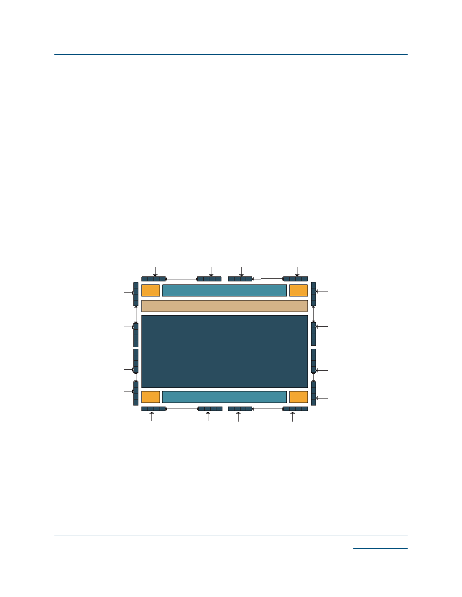
The two larger QL58x0 devices contain eight I/O banks. Figure 9 illustrates the I/O bank configurations for
QL5840. The two smaller QL58x0 devices contain two I/O banks per device. Figure 10 illustrates the I/O
bank configurations for QL5820 and QL5810.
Each I/O bank is independent of other I/O banks and each I/O bank has its own VCCIO and INREF supply
inputs. A mixture of different I/O standards can be used on the device; however, there is a limitation as to
which I/O standards can be supported within a given bank. Only standards that share a common VCCIO and
INREF can be shared within the same bank (e.g., PCI and LVTTL). In the case of the QL5820 and QL5810,
only one voltage-referenced standard can be used. The two I/O banks, A and B, share the INREF pin.
Figure 9: Multiple I/O Banks on QL5840
Embedded RAM Blocks
PLL
Fabric
Embeded Computational Units
Embedded RAM Blocks
PLL
VCCIO(F)
INREF(F)
VCCIO(E)
INREF(E)
VCCIO(D)
INREF(D)
VCCIO(C)
INREF (C)
INREF(B)
VCCIO(B)
INREF(A)
VCCIO(A)
INREF(H)
VCCIO(H)
INREF(G)
VCCIO(G)
相关PDF资料 |
PDF描述 |
|---|---|
| QL5820-33BPTN196C | PCI BUS CONTROLLER, PBGA196 |
| QL5842-33BPSN484M | PCI BUS CONTROLLER, PBGA484 |
| QT83C154XXX-L | 8-BIT, MROM, 6 MHz, MICROCONTROLLER, PQFP44 |
| QC87C251SQ | 8-BIT, UVPROM, 12 MHz, MICROCONTROLLER, CDIP40 |
| QR80C51XXX:R | 8-BIT, MROM, 12 MHz, MICROCONTROLLER, CQCC44 |
相关代理商/技术参数 |
参数描述 |
|---|---|
| QL5822-33BPTN280C-5695 | 制造商:QuickLogic Corporation 功能描述: |
| QL62506PB516C | 制造商:QUICK LOG 功能描述:New |
| QL6325PQ208 | 制造商:未知厂家 制造商全称:未知厂家 功能描述:ASIC |
| QL6325PT280 | 制造商:未知厂家 制造商全称:未知厂家 功能描述:ASIC |
| QL63D5SA | 制造商:未知厂家 制造商全称:未知厂家 功能描述:InGaAlP Laser Diode |
发布紧急采购,3分钟左右您将得到回复。