- 您现在的位置:买卖IC网 > PDF目录192295 > S29CD032J1JFAI122 (SPANSION LLC) 1M X 32 FLASH 2.7V PROM, 54 ns, PBGA80 PDF资料下载
参数资料
| 型号: | S29CD032J1JFAI122 |
| 厂商: | SPANSION LLC |
| 元件分类: | PROM |
| 英文描述: | 1M X 32 FLASH 2.7V PROM, 54 ns, PBGA80 |
| 封装: | 13 X 11 MM, 1 MM PITCH, FORTIFIED, BGA-80 |
| 文件页数: | 22/78页 |
| 文件大小: | 1825K |
| 代理商: | S29CD032J1JFAI122 |
第1页第2页第3页第4页第5页第6页第7页第8页第9页第10页第11页第12页第13页第14页第15页第16页第17页第18页第19页第20页第21页当前第22页第23页第24页第25页第26页第27页第28页第29页第30页第31页第32页第33页第34页第35页第36页第37页第38页第39页第40页第41页第42页第43页第44页第45页第46页第47页第48页第49页第50页第51页第52页第53页第54页第55页第56页第57页第58页第59页第60页第61页第62页第63页第64页第65页第66页第67页第68页第69页第70页第71页第72页第73页第74页第75页第76页第77页第78页
September 27, 2006 S29CD-J_CL-J_00_B1
S29CD-J & S29CL-J Flash Family
27
Pr el im i n a r y
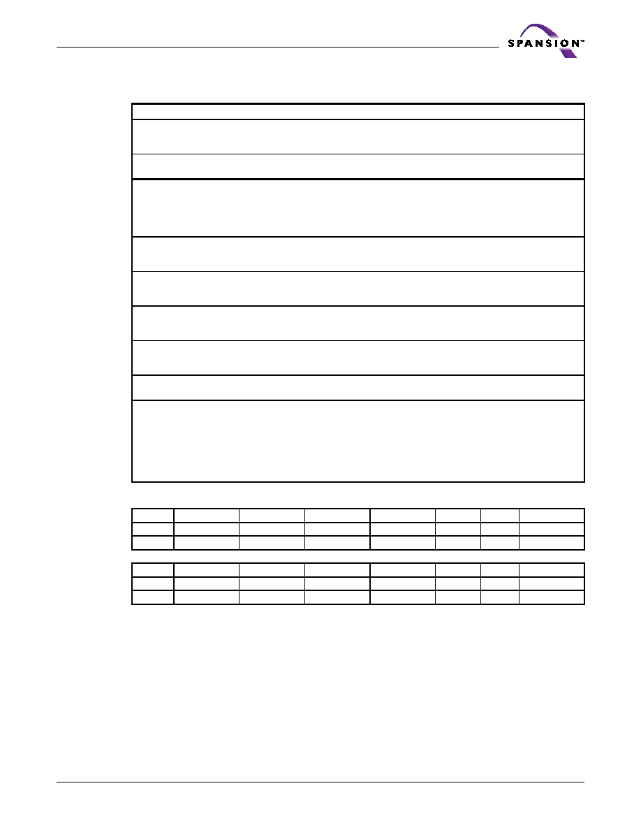
Table 8.5 describes the Configuration Register settings.
8.5
Autoselect
The autoselect mode provides manufacturer and device identification, and sector protection ver-
ification, through identifier codes output on DQ7–DQ0. This mode is primarily intended for
programming equipment to automatically match a device to be programmed with its correspond-
ing programming algorithm. However, the autoselect codes can also be accessed in-system
through the command register.
When using programming equipment, the autoselect mode requires VID on address pin A9. Ad-
dress pins A6, A1, and A0 must be as shown in Table 8.7. In addition, when verifying sector pro-
tection, the sector address must appear on the appropriate highest order address bits. Table 8.7
Table 8.5 Configuration Register
Configuration Register
CR15 = Read Mode (RM)
0 = Synchronous Burst Reads Enabled
1 = Asynchronous Reads Enabled (Default)
CR14 = Reserved for Future Enhancements
These bits are reserved for future use. Set these bits to 0.
CR13–CR10 = Initial Burst Access Delay Configuration (IAD3-IAD0)
0000 = 2 CLK cycle initial burst access delay
0001 = 3 CLK cycle initial burst access delay
0010 = 4 CLK cycle initial burst access delay
0011 = 5 CLK cycle initial burst access delay
0100 = 6 CLK cycle initial burst access delay
0101 = 7 CLK cycle initial burst access delay
0110 = 8 CLK cycle initial burst access delay
0111 = 9 CLK cycle initial burst access delay—Default
CR9 = Data Output Configuration (DOC)
0 = Hold Data for 1-CLK cycle—Default
1 = Reserved
CR8 = IND/WAIT# Configuration (WC)
0 = IND/WAIT# Asserted During Delay—Default
1 = IND/WAIT# Asserted One Data Cycle Before Delay
CR7 = Burst Sequence (BS)
0 = Reserved
1 = Linear Burst Order—Default
CR6 = Clock Configuration (CC)
0 = Reserved
1 = Burst Starts and Data Output on Rising Clock Edge—Default
CR5–CR3 = Reserved For Future Enhancements (R)
These bits are reserved for future use. Set these bits to 0.
CR2–CR0 = Burst Length (BL2–BL0)
000 = Reserved, burst accesses disabled (asynchronous reads only)
001 = 64 bit (8-byte) Burst Data Transfer - x32 Linear
010 = 128 bit (16-byte) Burst Data Transfer - x32 Linear
011 = 256 bit (32-byte) Burst Data Transfer - x32 Linear (device default)
100 = Reserved, burst accesses disabled (asynchronous reads only)
101 = Reserved, burst accesses disabled (asynchronous reads only)
110 = Reserved, burst accesses disabled (asynchronous reads only)
Table 8.6 Configuration Register After Device Reset
CR15
CR14
CR13
CR12
CR11
CR10
CR9
CR8
RM
Reserve
IAD3
IAD2
IAD1
IAD0
DOC
Reserve
1
0011
1
0
CR7
CR6
CR5
CR4
CR3
CR2
CR1
CR0
BS
CC
Reserve
BL2
BL1
BL0
1
1000
1
0
相关PDF资料 |
PDF描述 |
|---|---|
| S29CD032J1MFAN120 | 1M X 32 FLASH 2.7V PROM, 54 ns, PBGA80 |
| S29CD032J1MQFN133 | 1M X 32 FLASH 2.7V PROM, 54 ns, PQFP80 |
| S29CL016J0JQFI100 | 512K X 32 FLASH 3.3V PROM, 54 ns, PQFP80 |
| S29CL016J0MFAI113 | 512K X 32 FLASH 3.3V PROM, 54 ns, PBGA80 |
| S29CL016J0PQFI102 | 512K X 32 FLASH 3.3V PROM, 54 ns, PQFP80 |
相关代理商/技术参数 |
参数描述 |
|---|---|
| S29CL016J0JQFM030 | 制造商:Spansion 功能描述:FLASH PARALLEL 3.3V 16MBIT 512KX32 54NS 80PQFP - Trays |
| S29CL016J0JQFM030P | 制造商:Spansion 功能描述:AUTO 3.3V 512KX32 FLASH - Trays |
| S29CL016J0JQFM030U | 制造商:Spansion 功能描述:32M (4MX8/2MX16) 3V REG, MIRRORBIT, TOP, FBGA48, IND - Trays |
| S29CL016J0JQFM03U | 制造商:Spansion 功能描述:32M (4MX8/2MX16) 3V REG, MIRRORBIT, TOP, FBGA48, IND - Trays |
| S29CL016J0MQFM030 | 制造商:Spansion 功能描述: |
发布紧急采购,3分钟左右您将得到回复。