- 您现在的位置:买卖IC网 > PDF目录271233 > S29CD032J1MFAI020 (SPANSION LLC) 1M X 32 FLASH 2.7V PROM, 54 ns, PBGA80 PDF资料下载
参数资料
| 型号: | S29CD032J1MFAI020 |
| 厂商: | SPANSION LLC |
| 元件分类: | PROM |
| 英文描述: | 1M X 32 FLASH 2.7V PROM, 54 ns, PBGA80 |
| 封装: | 13 X 11 MM, 1 MM PITCH, FORTIFIED, BGA-80 |
| 文件页数: | 16/78页 |
| 文件大小: | 1825K |
| 代理商: | S29CD032J1MFAI020 |
第1页第2页第3页第4页第5页第6页第7页第8页第9页第10页第11页第12页第13页第14页第15页当前第16页第17页第18页第19页第20页第21页第22页第23页第24页第25页第26页第27页第28页第29页第30页第31页第32页第33页第34页第35页第36页第37页第38页第39页第40页第41页第42页第43页第44页第45页第46页第47页第48页第49页第50页第51页第52页第53页第54页第55页第56页第57页第58页第59页第60页第61页第62页第63页第64页第65页第66页第67页第68页第69页第70页第71页第72页第73页第74页第75页第76页第77页第78页
September 27, 2006 S29CD-J_CL-J_00_B1
S29CD-J & S29CL-J Flash Family
21
Pr el im i n a r y
8.2
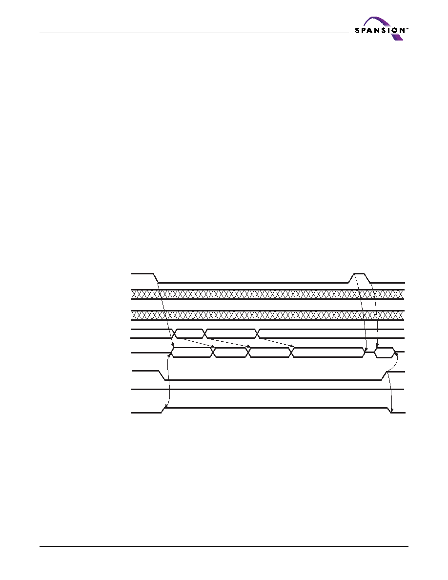
Asynchronous Read
All memories require access time to output array data. In an asynchronous read operation, data
is read from one memory location at a time. Addresses are presented to the device in random
order, and the propagation delay through the device causes the data on its outputs to arrive
asynchronously with the address on its inputs.
The internal state machine is set for asynchronously reading array data upon device power-up,
or after a hardware reset. This ensures that no spurious alteration of the memory content occurs
during the power transition. No command is necessary in this mode to obtain array data. Stan-
dard microprocessor read cycles that assert valid addresses on the device address inputs
produce valid data on the device data outputs. The device remains enabled for read access until
the command register contents are altered.
The device has two control functions which must be satisfied in order to obtain data at the out-
puts. CE# is the power control and should be used for device selection (CE# must be set to VIL
to read data). OE# is the output control and should be used to gate data to the output pins if
the device is selected (OE# must be set to VIL in order to read data). WE# should remain at VIH
(when reading data).
Address access time (tACC) is equal to the delay from stable addresses to valid output data. The
chip enable access time (tCE) is the delay from the stable addresses and stable CE# to valid data
at the output pins. The output enable access time (tOE) is the delay from the falling edge of OE#
to valid data at the output pins (assuming the addresses have been stable for at least a period
diagram of an asynchronous read operation.
Note: Operation is shown for the 32-bit data bus. For the 16-bit data bus, A-1 is required.
Figure 8.1 Asynchronous Read Operation
Refer to Asynchronous Operations on page 56 for timing specifications and to Figure 18.2, Con-
ventional Read Operations Timings, on page 56 for another timing diagram. ICC1 in the DC
Characteristics table represents the active current specification for reading array data.
D0
D1
D2
D3
CE#
CLK
ADV#
Addresses
Data
OE#
WE#
IND/WAIT#
VIH
Float
VOH
Address 0
Address 1
Address 2
Address 3
Float
相关PDF资料 |
PDF描述 |
|---|---|
| S29CL016J0JFAI112 | 512K X 32 FLASH 3.3V PROM, 54 ns, PBGA80 |
| S29CL016J0JFFI130 | 512K X 32 FLASH 3.3V PROM, 54 ns, PBGA80 |
| S29CL016J0MQAI113 | 512K X 32 FLASH 3.3V PROM, 54 ns, PQFP80 |
| S29CL016J0PQFI123 | 512K X 32 FLASH 3.3V PROM, 54 ns, PQFP80 |
| S29CL016J1MFAI123 | 512K X 32 FLASH 3.3V PROM, 54 ns, PBGA80 |
相关代理商/技术参数 |
参数描述 |
|---|---|
| S29CL016J0JQFM030 | 制造商:Spansion 功能描述:FLASH PARALLEL 3.3V 16MBIT 512KX32 54NS 80PQFP - Trays |
| S29CL016J0JQFM030P | 制造商:Spansion 功能描述:AUTO 3.3V 512KX32 FLASH - Trays |
| S29CL016J0JQFM030U | 制造商:Spansion 功能描述:32M (4MX8/2MX16) 3V REG, MIRRORBIT, TOP, FBGA48, IND - Trays |
| S29CL016J0JQFM03U | 制造商:Spansion 功能描述:32M (4MX8/2MX16) 3V REG, MIRRORBIT, TOP, FBGA48, IND - Trays |
| S29CL016J0MQFM030 | 制造商:Spansion 功能描述: |
发布紧急采购,3分钟左右您将得到回复。