- 您现在的位置:买卖IC网 > PDF目录271233 > S29CD032J1MFAI020 (SPANSION LLC) 1M X 32 FLASH 2.7V PROM, 54 ns, PBGA80 PDF资料下载
参数资料
| 型号: | S29CD032J1MFAI020 |
| 厂商: | SPANSION LLC |
| 元件分类: | PROM |
| 英文描述: | 1M X 32 FLASH 2.7V PROM, 54 ns, PBGA80 |
| 封装: | 13 X 11 MM, 1 MM PITCH, FORTIFIED, BGA-80 |
| 文件页数: | 24/78页 |
| 文件大小: | 1825K |
| 代理商: | S29CD032J1MFAI020 |
第1页第2页第3页第4页第5页第6页第7页第8页第9页第10页第11页第12页第13页第14页第15页第16页第17页第18页第19页第20页第21页第22页第23页当前第24页第25页第26页第27页第28页第29页第30页第31页第32页第33页第34页第35页第36页第37页第38页第39页第40页第41页第42页第43页第44页第45页第46页第47页第48页第49页第50页第51页第52页第53页第54页第55页第56页第57页第58页第59页第60页第61页第62页第63页第64页第65页第66页第67页第68页第69页第70页第71页第72页第73页第74页第75页第76页第77页第78页
28
S29CD-J & S29CL-J Flash Family
S29CD-J_CL-J_00_B1 September27,2006
Prel imi n ary
shows the remaining address bits that are don’t care. When all necessary bits have been set as
required, the programming equipment may then read the corresponding identifier code on DQ7–
DQ0.
In order to access the autoselect codes in-system, the host system can issue the autoselect com-
mand via the command. This method does not require VID. See Command Definitions on
page 71 for details on using the autoselect mode. Autoselect mode can be used in either syn-
chronous (Burst) mode or asynchronous (Non Burst) mode.
The system must write the reset command to exit the autoselect mode and return to reading the
array data. See Table 8.7 for command sequence details.
Legend: L = Logic Low = VIL, H = Logic High = VIH, SA = Sector Address, X = Don’t care.
Note: The autoselect codes can also be accessed in-system via command sequences. See Table 20.2.
8.6
VersatileI/O (VIO) Control
The VersatileI/O (VIO) control allows the host system to set the voltage levels that the device
generates at its data outputs and the voltages tolerated at its data inputs to the same voltage
level that is asserted on the VIO pin. The output voltage generated on the device is determined
based on the VIO (VCCQ) level. For the 2.6 V (CD-J), a VIO of 1.65 V - 3.6 V (CD032J has a VIO
of 1.65V to 2.75V) allows the device to interface with I/Os lower than 2.5 V. For a 3.3 V VCC (CL-
J), a VIO of 1.65 V-3.60 V allows the device to interface with I/Os lower than 3.0 V.
8.7
Program/Erase Operations
These devices are capable of several modes of programming and or erase operations which are
described in detail in the following sections. However, prior to any programming and or erase
operation, devices must be set up appropriately as outlined in the configuration register
(Table 8.5 on page 27). During a synchronous write operation, to write a command or command
sequence (including programming data to the device and erasing sectors of memory), the sys-
tem must drive AVD# and CE# to VIL, and OE# to VIH when providing an address to the device,
and drive WE# and CE# to VIL, and OE# to VIH when writing commands or programming data.
8.7.1
Programming
Programming is a four-bus-cycle operation. The program command sequence is initiated by writ-
ing two unlock write cycles, followed by the program setup command. The program address and
data are written next, which in turn initiate the Embedded Program algorithm. The system is not
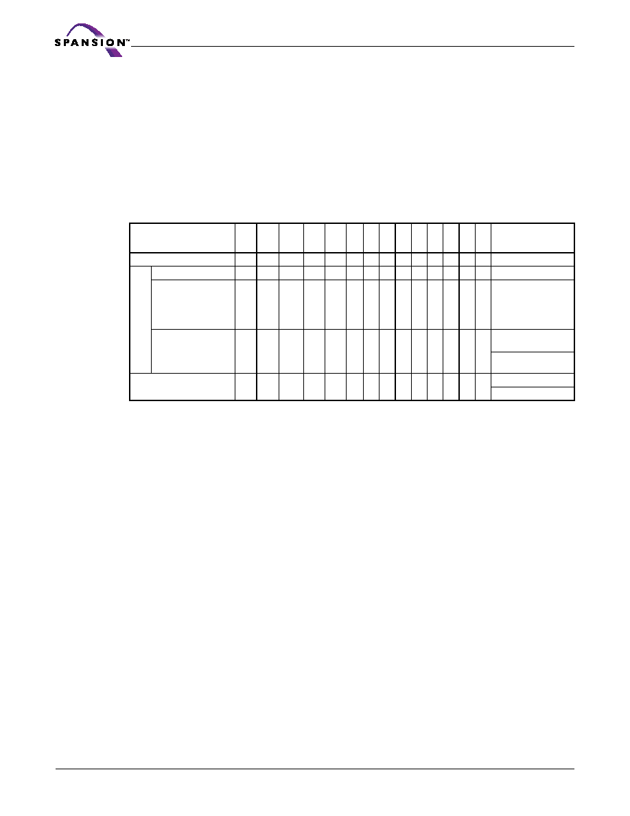
Table 8.7 S29CD-J & S29CL-J Flash Family Autoselect Codes (High Voltage Method)
Description
CE# OE# WE#
A19
to
A11
A10 A9 A8 A7 A6
A5
to
A4
A3 A2 A1 A0
DQ7
to
DQ0
Manufacturer ID: Spansion
LL
H
X
VID X
X
L
X
L
0001h
Au
to
se
le
ct
De
vi
ce
Co
de
Read Cycle 1
LL
H
X
VID X
L
X
L
H
007Eh
Read Cycle 2
LL
H
X
VID X
LLL
H
L
08h or 36h for
CD016J
46h for CL016J
09h for CD032J
49h for CL032J
Read Cycle 3
LL
H
X
VID X
L
HHHH
0000h
Top Boot Option
0001h
Bottom Boot Option
PPB Protection Status
LL
H
SA
X
VID X
LLLLL
H
L
0000h (unprotected)
0001h (protected)
相关PDF资料 |
PDF描述 |
|---|---|
| S29CL016J0JFAI112 | 512K X 32 FLASH 3.3V PROM, 54 ns, PBGA80 |
| S29CL016J0JFFI130 | 512K X 32 FLASH 3.3V PROM, 54 ns, PBGA80 |
| S29CL016J0MQAI113 | 512K X 32 FLASH 3.3V PROM, 54 ns, PQFP80 |
| S29CL016J0PQFI123 | 512K X 32 FLASH 3.3V PROM, 54 ns, PQFP80 |
| S29CL016J1MFAI123 | 512K X 32 FLASH 3.3V PROM, 54 ns, PBGA80 |
相关代理商/技术参数 |
参数描述 |
|---|---|
| S29CL016J0JQFM030 | 制造商:Spansion 功能描述:FLASH PARALLEL 3.3V 16MBIT 512KX32 54NS 80PQFP - Trays |
| S29CL016J0JQFM030P | 制造商:Spansion 功能描述:AUTO 3.3V 512KX32 FLASH - Trays |
| S29CL016J0JQFM030U | 制造商:Spansion 功能描述:32M (4MX8/2MX16) 3V REG, MIRRORBIT, TOP, FBGA48, IND - Trays |
| S29CL016J0JQFM03U | 制造商:Spansion 功能描述:32M (4MX8/2MX16) 3V REG, MIRRORBIT, TOP, FBGA48, IND - Trays |
| S29CL016J0MQFM030 | 制造商:Spansion 功能描述: |
发布紧急采购,3分钟左右您将得到回复。