- 您现在的位置:买卖IC网 > PDF目录271233 > S29CD032J1MFAI020 (SPANSION LLC) 1M X 32 FLASH 2.7V PROM, 54 ns, PBGA80 PDF资料下载
参数资料
| 型号: | S29CD032J1MFAI020 |
| 厂商: | SPANSION LLC |
| 元件分类: | PROM |
| 英文描述: | 1M X 32 FLASH 2.7V PROM, 54 ns, PBGA80 |
| 封装: | 13 X 11 MM, 1 MM PITCH, FORTIFIED, BGA-80 |
| 文件页数: | 21/78页 |
| 文件大小: | 1825K |
| 代理商: | S29CD032J1MFAI020 |
第1页第2页第3页第4页第5页第6页第7页第8页第9页第10页第11页第12页第13页第14页第15页第16页第17页第18页第19页第20页当前第21页第22页第23页第24页第25页第26页第27页第28页第29页第30页第31页第32页第33页第34页第35页第36页第37页第38页第39页第40页第41页第42页第43页第44页第45页第46页第47页第48页第49页第50页第51页第52页第53页第54页第55页第56页第57页第58页第59页第60页第61页第62页第63页第64页第65页第66页第67页第68页第69页第70页第71页第72页第73页第74页第75页第76页第77页第78页
26
S29CD-J & S29CL-J Flash Family
S29CD-J_CL-J_00_B1 September27,2006
Prel imi n ary
Notes:
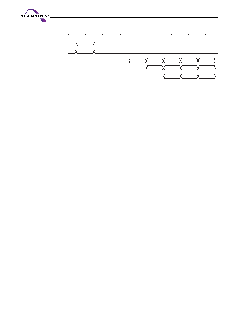
1. Burst access starts with a rising CLK edge and when ADV# is active.
2. Configurations register 6 is always set to 1 (CR6 = 1). Burst starts and data outputs on the rising CLK edge.
3. CR [13-10] = 1 or three clock cycles
4. CR [13-10] = 2 or four clock cycles
5. CR [13-10] = 3 or five clock cycles
Figure 8.4 Initial Burst Delay Control
8.4.3
Configuration Register
The configuration register sets various operational parameters associated with burst mode. Upon
power-up or hardware reset, the device defaults to the asynchronous read mode and the con-
figuration register settings are in their default state. (See Table 8.6 for the default Configuration
Register settings.) The host system determines the proper settings for the entire configuration
register, and then execute the Set Configuration Register command sequence before attempting
burst operations. The configuration register is not reset after deasserting CE#.
The Configuration Register does not occupy any addressable memory location, but rather, is ac-
cessed by the Configuration Register commands. The Configuration Register is readable at any
time, however, writing the Configuration Register is restricted to times when the Embedded Al-
gorithm is not active. If the user attempts to write the Configuration Register while the
Embedded Algorithm is active, the write operation is ignored and the contents of the Configu-
ration Register remain unchanged.
The Configuration Register is a 16 bit data field which is accessed by DQ15–DQ0. During a read
operation, DQ31–DQ16 returns all zeroes. Also, the Configuration Register reads operate the
same as the Autoselect command reads. When the command is issued, the bank address is
latched along with the command. Read operations to the bank that was specified during the Con-
figuration Register read command return Configuration Register contents. Read operations to the
other bank return flash memory data. Either bank address is permitted when writing the Config-
uration Register read command.
The configuration register can be read with a four-cycle command sequence. See Command Def-
initions on page 71 for sequence details.
CLK
ADV#
Addresses
DQ31-DQ03
DQ31-DQ04
DQ31-DQ05
Valid Address
Three CLK Delay
2nd CLK
3rd CLK
4th CLK
5th CLK
1st CLK
Four CLK Delay
Address 1 Latched
Five CLK Delay
D0
D1
D2
D3
D0
D1
D2
D0
D1
D2
D3
D4
相关PDF资料 |
PDF描述 |
|---|---|
| S29CL016J0JFAI112 | 512K X 32 FLASH 3.3V PROM, 54 ns, PBGA80 |
| S29CL016J0JFFI130 | 512K X 32 FLASH 3.3V PROM, 54 ns, PBGA80 |
| S29CL016J0MQAI113 | 512K X 32 FLASH 3.3V PROM, 54 ns, PQFP80 |
| S29CL016J0PQFI123 | 512K X 32 FLASH 3.3V PROM, 54 ns, PQFP80 |
| S29CL016J1MFAI123 | 512K X 32 FLASH 3.3V PROM, 54 ns, PBGA80 |
相关代理商/技术参数 |
参数描述 |
|---|---|
| S29CL016J0JQFM030 | 制造商:Spansion 功能描述:FLASH PARALLEL 3.3V 16MBIT 512KX32 54NS 80PQFP - Trays |
| S29CL016J0JQFM030P | 制造商:Spansion 功能描述:AUTO 3.3V 512KX32 FLASH - Trays |
| S29CL016J0JQFM030U | 制造商:Spansion 功能描述:32M (4MX8/2MX16) 3V REG, MIRRORBIT, TOP, FBGA48, IND - Trays |
| S29CL016J0JQFM03U | 制造商:Spansion 功能描述:32M (4MX8/2MX16) 3V REG, MIRRORBIT, TOP, FBGA48, IND - Trays |
| S29CL016J0MQFM030 | 制造商:Spansion 功能描述: |
发布紧急采购,3分钟左右您将得到回复。