- 您现在的位置:买卖IC网 > PDF目录192297 > S29GL032M10BAIR42 (SPANSION LLC) Conductive Polymer Chip Capacitors / T520 Series - High Temperature; Capacitance [nom]: 33uF; Working Voltage (Vdc)[max]: 6.3V; Capacitance Tolerance: +/-20%; Dielectric: Conductive Polymer; Lead Style: Surface-Mount Chip; Lead Dimensions: 3528-21; Termination: Solder Coated (SnPb, Pb 5% min); Body Dimensions: 3.5mm x 2.8mm x 1.9mm; Temperature Range: -55C to +125C; Container: Tape & Reel; Qty per Container: 2,000; Features: Low Temperature PDF资料下载
参数资料
| 型号: | S29GL032M10BAIR42 |
| 厂商: | SPANSION LLC |
| 元件分类: | PROM |
| 英文描述: | Conductive Polymer Chip Capacitors / T520 Series - High Temperature; Capacitance [nom]: 33uF; Working Voltage (Vdc)[max]: 6.3V; Capacitance Tolerance: +/-20%; Dielectric: Conductive Polymer; Lead Style: Surface-Mount Chip; Lead Dimensions: 3528-21; Termination: Solder Coated (SnPb, Pb 5% min); Body Dimensions: 3.5mm x 2.8mm x 1.9mm; Temperature Range: -55C to +125C; Container: Tape & Reel; Qty per Container: 2,000; Features: Low Temperature |
| 中文描述: | 2M X 16 FLASH 3V PROM, 100 ns, PBGA48 |
| 封装: | 8 X 9 MM, FBGA-48 |
| 文件页数: | 34/116页 |
| 文件大小: | 6024K |
| 代理商: | S29GL032M10BAIR42 |
第1页第2页第3页第4页第5页第6页第7页第8页第9页第10页第11页第12页第13页第14页第15页第16页第17页第18页第19页第20页第21页第22页第23页第24页第25页第26页第27页第28页第29页第30页第31页第32页第33页当前第34页第35页第36页第37页第38页第39页第40页第41页第42页第43页第44页第45页第46页第47页第48页第49页第50页第51页第52页第53页第54页第55页第56页第57页第58页第59页第60页第61页第62页第63页第64页第65页第66页第67页第68页第69页第70页第71页第72页第73页第74页第75页第76页第77页第78页第79页第80页第81页第82页第83页第84页第85页第86页第87页第88页第89页第90页第91页第92页第93页第94页第95页第96页第97页第98页第99页第100页第101页第102页第103页第104页第105页第106页第107页第108页第109页第110页第111页第112页第113页第114页第115页第116页
22
S29GL-M MirrorBitTM Flash Family
S29GL-M_00_B8 February 7, 2007
Data
Sheet
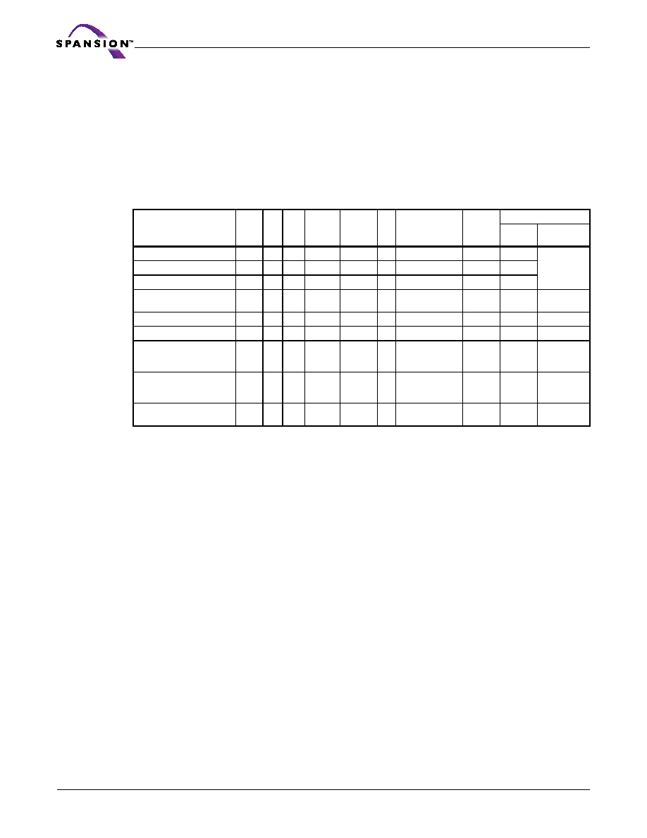
Device Bus Operations
This section describes the requirements and use of the device bus operations, which are initiated
through the internal command register. The command register itself does not occupy any addres-
sable memory location. The register is a latch used to store the commands, along with the
address and data information needed to execute the command. The contents of the register serve
as inputs to the internal state machine. The state machine outputs dictate the function of the de-
vice. Table 5 lists the device bus operations, the inputs and control levels they require, and the
resulting output. The following subsections describe each of these operations in further detail.
Legend: L = Logic Low = VIL, H = Logic High = VIH, VID = 11.5–12.5 V,
VHH = 11.5 V – 12.5 V, X = Don’t Care, SA = Sector Address, AIN = Address In,
DIN = Data In, DOUT = Data Out
Notes:
1. Addresses are Amax:A0 in word mode; Amax:A-1 in byte mode. Sector addresses are Amax:A15
in both modes.
2. The sector protect and sector unprotect functions may also be implemented via programming
equipment. See the “Sector Group Protection and Unprotection” section.
3. If WP# = VIL, the first or last sector remains protected (for uniform sector devices), and the two
outer boot sectors are protected (for boot sector devices). If WP# = VIH, the first or last sector, or
the two outer boot sectors are protected or unprotected as determined by the method described in
“Sector Group Protection and Unprotection”. All sectors are unprotected when shipped from the
factory (The Secured Silicon Sector may be factory protected depending on version ordered.)
4. DIN or DOUT as required by command sequence, data polling, or sector protect algorithm (see
Word/Byte Configuration
The BYTE# pin controls whether the device data I/O pins operate in the byte or word configura-
tion. If the BYTE# pin is set at logic ‘1’, the device is in word configuration, DQ0–DQ15 are active
and controlled by CE# and OE#.
If the BYTE# pin is set at logic ‘0’, the device is in byte configuration, and only data I/O pins DQ0–
DQ7 are active and controlled by CE# and OE#. The data I/O pins DQ8–DQ14 are tri-stated, and
the DQ15 pin is used as an input for the LSB (A-1) address function.
Requirements for Reading Array Data
To read array data from the outputs, the system must drive the CE# and OE# pins to VIL. CE# is
the power control and selects the device. OE# is the output control and gates array data to the
output pins. WE# should remain at VIH.
Table 5. Device Bus Operations
Operation
CE#
OE
#
WE# RESET#
WP#
AC
C
Addresses
DQ0–
DQ7
DQ8–DQ15
BYTE#
= VIH
BYTE#
= VIL
Read
LL
H
X
AIN
DOUT
DQ8–DQ14
= High-Z,
DQ15 = A-1
Write (Program/Erase)
LH
L
H
AIN
Accelerated Program
LH
L
H
AIN
Standby
VCC ±
0.3 V
XX
VCC ±
0.3 V
X
H
X
High-Z
Output Disable
L
H
X
High-Z
Reset
X
L
X
High-Z
Sector Group Protect
LH
L
VID
HX
SA, A6 =L,
A3=L, A2=L,
A1=H, A0=L
X
Sector Group Unprotect
LH
L
VID
HX
SA, A6=H,
A3=L, A2=L,
A1=H, A0=L
X
Temporary Sector
Group Unprotect
XX
X
VID
HX
AIN
(Note 4)(Note 4)High-Z
相关PDF资料 |
PDF描述 |
|---|---|
| S29GL032M10BAIR43 | MirrorBit Flash Family |
| S29GL032M10BFIR42 | MirrorBit Flash Family |
| S29GL032M10BFIR32 | T528 Series - I, M, Z Case Sizes - Face Down Termination Tantalum Surface Mount Capacitor; Capacitance [nom]: 330uF; Working Voltage (Vdc)[max]: 4V; Capacitance Tolerance: +/-20%; Dielectric: Tantalum, Solid; ESR: 9.0mΩ; Lead Style: Surface-Mount Chip; Lead Dimensions: 7343-17; Termination: 100% Tin (Sn); Body Dimensions: 7.3mm x 4.3mm x 1.7mm; Temperature Range: -55C to +105C; Container: Tape & Reel; Qty per Container: 1,000; Features: Face Down Termination |
| S29GL032M10BFIR40 | MirrorBit Flash Family |
| S29GL032M10TAIR00 | MirrorBit Flash Family |
相关代理商/技术参数 |
参数描述 |
|---|---|
| S29GL032M10BAIR43 | 制造商:SPANSION 制造商全称:SPANSION 功能描述:3.0 Volt-only Page Mode Flash Memory featuring 0.23 um MirrorBit process technology |
| S29GL032M10BAIR50 | 制造商:SPANSION 制造商全称:SPANSION 功能描述:MirrorBit Flash Family |
| S29GL032M10BAIR52 | 制造商:SPANSION 制造商全称:SPANSION 功能描述:MirrorBit Flash Family |
| S29GL032M10BAIR53 | 制造商:SPANSION 制造商全称:SPANSION 功能描述:MirrorBit Flash Family |
| S29GL032M10BAIR60 | 制造商:SPANSION 制造商全称:SPANSION 功能描述:MirrorBit Flash Family |
发布紧急采购,3分钟左右您将得到回复。