- 您现在的位置:买卖IC网 > PDF目录231009 > S71PL032J80BAW074 (SPANSION LLC) SPECIALTY MEMORY CIRCUIT, PBGA56 PDF资料下载
参数资料
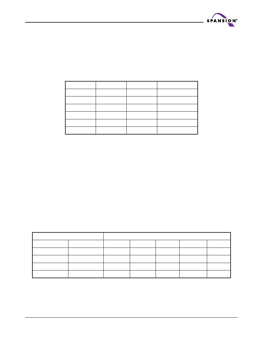
| 型号: | S71PL032J80BAW074 |
| 厂商: | SPANSION LLC |
| 元件分类: | 存储器 |
| 英文描述: | SPECIALTY MEMORY CIRCUIT, PBGA56 |
| 封装: | 7 X 9 MM, 1.20 MM HEIGHT, FBGA-56 |
| 文件页数: | 31/188页 |
| 文件大小: | 5078K |
| 代理商: | S71PL032J80BAW074 |
第1页第2页第3页第4页第5页第6页第7页第8页第9页第10页第11页第12页第13页第14页第15页第16页第17页第18页第19页第20页第21页第22页第23页第24页第25页第26页第27页第28页第29页第30页当前第31页第32页第33页第34页第35页第36页第37页第38页第39页第40页第41页第42页第43页第44页第45页第46页第47页第48页第49页第50页第51页第52页第53页第54页第55页第56页第57页第58页第59页第60页第61页第62页第63页第64页第65页第66页第67页第68页第69页第70页第71页第72页第73页第74页第75页第76页第77页第78页第79页第80页第81页第82页第83页第84页第85页第86页第87页第88页第89页第90页第91页第92页第93页第94页第95页第96页第97页第98页第99页第100页第101页第102页第103页第104页第105页第106页第107页第108页第109页第110页第111页第112页第113页第114页第115页第116页第117页第118页第119页第120页第121页第122页第123页第124页第125页第126页第127页第128页第129页第130页第131页第132页第133页第134页第135页第136页第137页第138页第139页第140页第141页第142页第143页第144页第145页第146页第147页第148页第149页第150页第151页第152页第153页第154页第155页第156页第157页第158页第159页第160页第161页第162页第163页第164页第165页第166页第167页第168页第169页第170页第171页第172页第173页第174页第175页第176页第177页第178页第179页第180页第181页第182页第183页第184页第185页第186页第187页第188页
May 4, 2004 pSRAM_Type07_13_A0
pSRAM Type 7
127
Prelimin ary
The default state is Sleep and it is the lowest power consumption but all data will
be lost once CE2 is brought to Low for Power Down. It is not required to program
to Sleep mode after power-up.
Power Down Program Sequence
The program requires total 6 read/write operation with unique address. Between
each read/write operation requires that device be in standby mode. Following
table shows the detail sequence.
The first cycle is to read from most significant address (MSB).
The second and third cycle are to write back the data (RDa) read by first cycle.
If the second or third cycle is written into the different address, the program is
cancelled and the data written by the second or third cycle is valid as a normal
write operation.
The forth and fifth cycle is to write to MSB. The data of forth and fifth cycle is
don’t-care. If the forth or fifth cycle is written into different address, the program
is also cancelled but write data may not be wrote as normal write operation.
The last cycle is to read from specific address key for mode selection.
Once this program sequence is performed from a Partial mode to the other Partial
mode, the written data stored in memory cell array may be lost. So, it should per-
form this program prior to regular read/write operation if Partial mode is used.
Address Key
The address key has following format.
Cycle #
Operation
Address
Data
1st
Read
3FFFFFh (MSB)
Read Data (RDa)
2nd
Write
3FFFFFh
RDa
3rd
Write
3FFFFFh
RDa
4th
Write
3FFFFFh
Don’t Care (X)
5th
Write
3FFFFFh
X
6th
Read
Address Key
Read Data (RDb)
Mode
Address
32M
64M
A21
A20
A19
A18 - A0
Binary
Sleep (default)
1
3FFFFFh
4M Partial
N/A
1
0
1
37FFFFh
8M Partial
1
0
1
2FFFFFh
N/A
16M Partial
1
0
1
27FFFFh
相关PDF资料 |
PDF描述 |
|---|---|
| S71PL032JA0BAW074 | SPECIALTY MEMORY CIRCUIT, PBGA56 |
| S71PL032JA0BFW0F4 | SPECIALTY MEMORY CIRCUIT, PBGA56 |
| S29JL032H60TAI023 | 2M X 16 FLASH 3V PROM, 60 ns, PDSO48 |
| S29AL016D70BAI022 | 1M X 16 FLASH 3V PROM, 70 ns, PBGA48 |
| S29AL016D70TAN013 | 1M X 16 FLASH 3V PROM, 70 ns, PDSO48 |
相关代理商/技术参数 |
参数描述 |
|---|---|
| S71PL032J80BAW0Z0 | 制造商:SPANSION 制造商全称:SPANSION 功能描述:Based MCPs |
| S71PL032J80BAW0Z2 | 制造商:SPANSION 制造商全称:SPANSION 功能描述:Based MCPs |
| S71PL032J80BAW0Z3 | 制造商:SPANSION 制造商全称:SPANSION 功能描述:Based MCPs |
| S71PL032J80BAW9Z0 | 制造商:SPANSION 制造商全称:SPANSION 功能描述:Based MCPs |
| S71PL032J80BAW9Z2 | 制造商:SPANSION 制造商全称:SPANSION 功能描述:Based MCPs |
发布紧急采购,3分钟左右您将得到回复。