- 您现在的位置:买卖IC网 > PDF目录19934 > SDIN2C2-2G (SanDisk)IC INAND FLASH 2GB 169FBGA PDF资料下载
参数资料
| 型号: | SDIN2C2-2G |
| 厂商: | SanDisk |
| 文件页数: | 4/29页 |
| 文件大小: | 0K |
| 描述: | IC INAND FLASH 2GB 169FBGA |
| 标准包装: | 112 |
| 格式 - 存储器: | 闪存 |
| 存储器类型: | 闪存 - NAND |
| 存储容量: | 16G(2G x 8) |
| 速度: | 50MHz |
| 接口: | SD/SPI 串行 |
| 电源电压: | 2.7 V ~ 3.6 V |
| 工作温度: | -25°C ~ 85°C |
| 封装/外壳: | 169-FBGA |
| 供应商设备封装: | 169-BGA(12x16) |
| 包装: | 托盘 |
| 其它名称: | 585-1229 |
第1页第2页第3页当前第4页第5页第6页第7页第8页第9页第10页第11页第12页第13页第14页第15页第16页第17页第18页第19页第20页第21页第22页第23页第24页第25页第26页第27页第28页第29页
�� �
�
�Chapter� 1� –� Introduction�
�Revision� 1.1�
�1�
�1.1�
�Introduction�
�General� Description�
�PRELIMINARY�
�SanDisk� iNAND� Product� Manual�
�The� SanDisk� iNAND� is� a� very� small,� flash� storage� device,� designed� specifically� for� storage�
�applications� that� put� a� premium� on� small� form� factor,� low� power� and� low� cost.� Flash� is� the�
�ideal� storage� medium� for� portable,� battery-powered� devices.� It� features� low� power�
�consumption� and� is� non-volatile,� requiring� no� power� to� maintain� the� stored� data.� It� also� has�
�a� wide� operating� range� for� temperature,� shock� and� vibration.� It� is� compatible� with� the� JC64�
�FBGA� 169,� 0.5mm� ball� pitch,� package.�
�SanDisk� iNAND� is� well-suited� to� meet� the� needs� of� small,� low� power,� electronic� devices.�
�With� form� factors� measuring� 12mm� x� 16mm� x� 1.2� mm� and� 12mm� x� 18mm� x� 1.2mm,�
�iNAND� is� expected� to� be� used� in� a� wide� variety� of� portable� devices� like� mobile� phones,�
�pagers,� and� voice� recorders.�
�To� support� this� wide� range� of� applications,� iNAND� is� offered� with� an� SD� Interface.� The� SD�
�interface� product� is� fully� compatible� with� iNAND� products,� and� provides� a� 4-bit� data� bus�
�for� maximum� performance.� For� compatibility� with� existing� controllers,� the� iNAND� offers,�
�in� addition� to� these� interfaces,� an� alternate� communication-protocol� based� on� the� SPI�
�standard.�
�These� interfaces� allow� for� easy� integration� into� any� design,� regardless� of� which� type� of�
�microprocessor� is� used.� All� device� and� interface� configuration� data� (such� as� maximum�
�frequency� and� card� identification)� are� stored� on� the� device.�
�The� SanDisk� iNAND� provides� up� to� 8� GB� of� memory� for� use� in� mass� storage� applications.�
�In� addition� to� the� mass-storage-specific� flash� memory� chip,� iNAND� includes� an� intelligent�
�controller,� which� manages� interface� protocols,� data� storage� and� retrieval,� error� correction�
�code� (ECC)� algorithms,� defect� handling� and� diagnostics,� power� management,� wear�
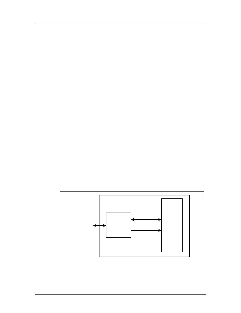
�leveling,� and� clock� control.� Figure� 1-1� is� a� block� diagram� of� the� SanDisk� iNAND� with� SD�
�Interface.�
�Figure� 1-1�
�SanDisk� iNAND� Block� Diagram�
�SanDisk� iNAND2�
�SD� Bus/SPI� Bus�
�Interface�
�?� 2007� SanDisk� Corporation�
�SanDisk�
�Single� Chip�
�Controller�
�1-1�
�Data� In/Out�
�Control�
�Flash�
�Memory�
�02/09/07�
�相关PDF资料 |
PDF描述 |
|---|---|
| VE-BN1-CV-S | CONVERTER MOD DC/DC 12V 150W |
| LTC4241IGN#TR | IC CTRLR HOTSWAP 3.3V AUX 20SSOP |
| SDIN2C2-1G | IC INAND FLASH 1GB 169FBGA |
| DS1258Y-70IND# | IC NVSRAM 2MBIT 70NS 40DIP |
| VE-2WF-CW-S | CONVERTER MOD DC/DC 72V 100W |
相关代理商/技术参数 |
参数描述 |
|---|---|
| SDIN2C2-2G-T | 功能描述:IC INAND FLASH 2GB 169FBGA RoHS:是 类别:集成电路 (IC) >> 存储器 系列:- 标准包装:150 系列:- 格式 - 存储器:EEPROMs - 串行 存储器类型:EEPROM 存储容量:4K (2 x 256 x 8) 速度:400kHz 接口:I²C,2 线串口 电源电压:2.5 V ~ 5.5 V 工作温度:-40°C ~ 85°C 封装/外壳:8-VFDFN 裸露焊盘 供应商设备封装:8-DFN(2x3) 包装:管件 产品目录页面:1445 (CN2011-ZH PDF) |
| SDIN2C2-8G | 制造商:SanDisk Corporation 功能描述:8GB, 169FBGA 12X16, OEM |
| SDIN3C2-16G | 制造商:SanDisk Corporation 功能描述:SDIN3C2-16G,169TFBGA 12X16,MMC |
| SDIN3C2-2G | 制造商:SanDisk Corporation 功能描述:SDIN3C2-2G,169 BGA,12X16 MMC,O |
| SDIN4C1-8G | 制造商:SanDisk Corporation 功能描述:SDIN4C1-8G,169FBGA 12X16,OEM |
发布紧急采购,3分钟左右您将得到回复。