- 您现在的位置:买卖IC网 > PDF目录9582 > SI5315B-C-GMR (Silicon Laboratories Inc)IC CLOCK MULT 8KHZ-125MHZ 36QFN PDF资料下载
参数资料
| 型号: | SI5315B-C-GMR |
| 厂商: | Silicon Laboratories Inc |
| 文件页数: | 10/54页 |
| 文件大小: | 0K |
| 描述: | IC CLOCK MULT 8KHZ-125MHZ 36QFN |
| 应用说明: | SI5315/17 Crystal Selection AppNote |
| 标准包装: | 250 |
| 系列: | DSPLL® |
| 类型: | 时钟/频率倍增器,抖动衰减器,多路复用器 |
| PLL: | 无 |
| 主要目的: | 以太网,SONET/SDH/PDH,电信 |
| 输入: | CML,CMOS,LVDS,LVPECL |
| 输出: | CML,CMOS,LVDS,LVPECL |
| 电路数: | 1 |
| 比率 - 输入:输出: | 2:2 |
| 差分 - 输入:输出: | 是/是 |
| 频率 - 最大: | 125MHz |
| 电源电压: | 1.71 V ~ 3.63 V |
| 工作温度: | -40°C ~ 85°C |
| 安装类型: | 表面贴装 |
| 封装/外壳: | 36-VFQFN 裸露焊盘 |
| 供应商设备封装: | 36-QFN(6x6) |
| 包装: | 带卷 (TR) |
第1页第2页第3页第4页第5页第6页第7页第8页第9页当前第10页第11页第12页第13页第14页第15页第16页第17页第18页第19页第20页第21页第22页第23页第24页第25页第26页第27页第28页第29页第30页第31页第32页第33页第34页第35页第36页第37页第38页第39页第40页第41页第42页第43页第44页第45页第46页第47页第48页第49页第50页第51页第52页第53页第54页
Si5315
18
Rev. 1.0
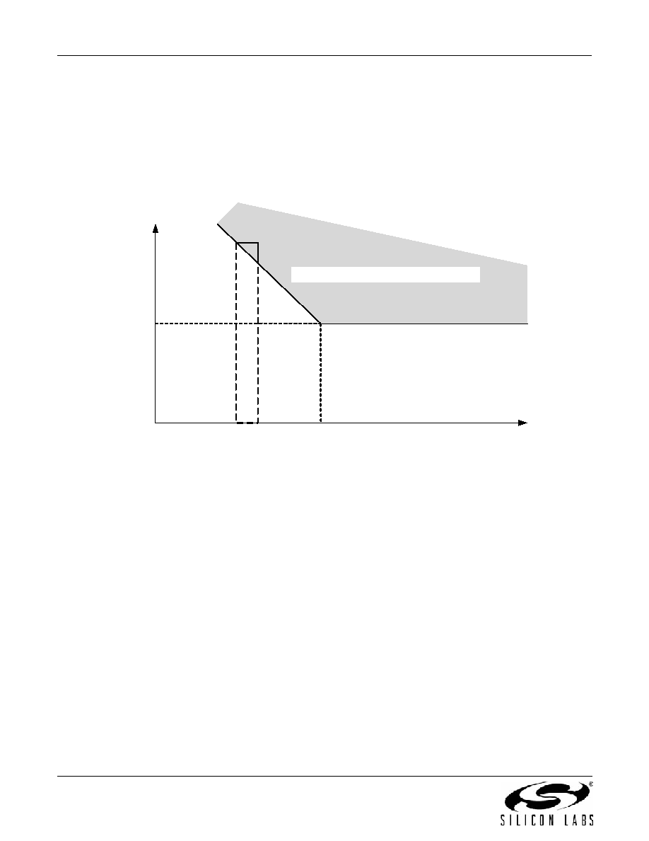
4.2.3. Jitter Tolerance
Jitter tolerance is defined as the maximum peak-to-peak sinusoidal jitter that can be present on the incoming clock
before the DSPLL loses lock. The tolerance is a function of the jitter frequency, because tolerance improves for
lower input jitter frequency.
The jitter tolerance of the DSPLL is a function of the loop bandwidth setting. Figure 9 shows the general shape of
the jitter tolerance curve versus input jitter frequency. For jitter frequencies above the loop bandwidth, the tolerance
is a constant value Aj0. Beginning at the PLL bandwidth, the tolerance increases at a rate of 20 dB/decade for
lower input jitter frequencies.
Figure 9. Jitter Tolerance Mask/Template
The equation for the high frequency jitter tolerance can be expressed as a function of the PLL loop bandwidth
(i.e., BW):
For example, the jitter tolerance when fin = 19.44 MHz, fout = 161.13 MHz and the loop bandwidth (BW) is 113 Hz:
4.2.4. Jitter Attenuation Performance
The Internal VCO uses the reference clock on the XA/XB pins as its reference for jitter attenuation. The XA/XB pins
support either a crystal input or an input buffer single-ended or differential clock input, such that an external
oscillator can become the reference source. In either case, the device accepts a wide margin in absolute frequency
of the reference input. (See 5.5. "Holdover Mode" on page 32.) In holdover, the Si5315's output clock stability
matches the reference supplied on the XA/XB pins. The external crystal or reference clock must be selected based
on the stability requirements of the application if holdover is a key requirement.
However, care must be exercised in certain areas for optimum performance. For examples of connections to the
XA/XB pins, refer to 7. "Crystal/Reference Clock Input" on page 38.
Input
Jitter
Amplitude
Aj0
–20 dB/dec.
fJitter In
Excessive Input Jitter Range
BW/100 BW/10
BW
A
j0
5000
BW
------------- ns pk-pk
=
A
j0
5000
113
-------------
44.24 ns pk-pk
==
相关PDF资料 |
PDF描述 |
|---|---|
| VE-B5N-IU | CONVERTER MOD DC/DC 18.5V 200W |
| VI-2NZ-MY-S | CONVERTER MOD DC/DC 2V 20W |
| VE-B5M-IU | CONVERTER MOD DC/DC 10V 200W |
| VI-2NZ-MX-S | CONVERTER MOD DC/DC 2V 30W |
| MC1489AMG | IC LINE RECEIVER QUAD 14-SOEIAJ |
相关代理商/技术参数 |
参数描述 |
|---|---|
| SI5315-C | 制造商:AUK 制造商全称:AUK corp 功能描述:IRED |
| SI5315-C(B) | 制造商:AUK 制造商全称:AUK corp 功能描述:IRED |
| SI5315-C_1 | 制造商:AUK 制造商全称:AUK corp 功能描述:IRED |
| SI5315-CB | 制造商:AUK 制造商全称:AUK corp 功能描述:IRED |
| SI5315-DS | 制造商:AUK 制造商全称:AUK corp 功能描述:High Speed IRED |
发布紧急采购,3分钟左右您将得到回复。