- 您现在的位置:买卖IC网 > PDF目录9582 > SI5315B-C-GMR (Silicon Laboratories Inc)IC CLOCK MULT 8KHZ-125MHZ 36QFN PDF资料下载
参数资料
| 型号: | SI5315B-C-GMR |
| 厂商: | Silicon Laboratories Inc |
| 文件页数: | 8/54页 |
| 文件大小: | 0K |
| 描述: | IC CLOCK MULT 8KHZ-125MHZ 36QFN |
| 应用说明: | SI5315/17 Crystal Selection AppNote |
| 标准包装: | 250 |
| 系列: | DSPLL® |
| 类型: | 时钟/频率倍增器,抖动衰减器,多路复用器 |
| PLL: | 无 |
| 主要目的: | 以太网,SONET/SDH/PDH,电信 |
| 输入: | CML,CMOS,LVDS,LVPECL |
| 输出: | CML,CMOS,LVDS,LVPECL |
| 电路数: | 1 |
| 比率 - 输入:输出: | 2:2 |
| 差分 - 输入:输出: | 是/是 |
| 频率 - 最大: | 125MHz |
| 电源电压: | 1.71 V ~ 3.63 V |
| 工作温度: | -40°C ~ 85°C |
| 安装类型: | 表面贴装 |
| 封装/外壳: | 36-VFQFN 裸露焊盘 |
| 供应商设备封装: | 36-QFN(6x6) |
| 包装: | 带卷 (TR) |
第1页第2页第3页第4页第5页第6页第7页当前第8页第9页第10页第11页第12页第13页第14页第15页第16页第17页第18页第19页第20页第21页第22页第23页第24页第25页第26页第27页第28页第29页第30页第31页第32页第33页第34页第35页第36页第37页第38页第39页第40页第41页第42页第43页第44页第45页第46页第47页第48页第49页第50页第51页第52页第53页第54页
Si5315
16
Rev. 1.0
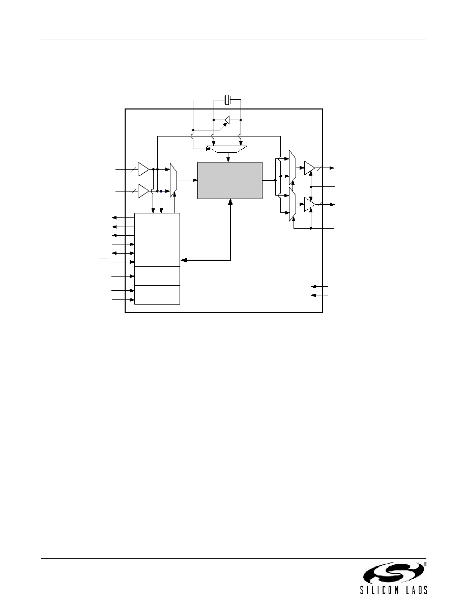
4. Functional Description
Figure 7. Detailed Block Diagram
4.1. Overview
The Si5315 is a jitter-attenuating precision clock multiplier for Synchronous Ethernet, SONET/SDH, and PDH
(T1/E1) applications. The Si5315 accepts dual clock inputs ranging from 8 kHz to 644.53 MHz and generates two
frequency-multiplied clock outputs ranging from 8 kHz to 644.53 MHz. The two input clocks are at the same
frequency and the two output clocks are at the same frequency. The input clock frequency and clock multiplication
ratio are selectable from a look up table of popular SyncE and T1/E1 rates.
The Si5315 is based on Silicon Laboratories' 3rd-generation DSPLL technology, which provides any-frequency
synthesis and jitter attenuation in a highly integrated PLL solution that eliminates the need for external VCXO and
loop filter components. The Si5315 PLL loop bandwidth is selectable via the BWSEL[1:0] pins and supports a
range from 60 to 8.4 kHz.
The Si5315 supports hitless switching between the two input clocks in compliance with ITU-T G.8262 and Telcordia
GR-253-CORE and GR-1244-CORE. This feature greatly minimizes the propagation of phase transients to the
clock outputs during an input clock transition (<200 ps typ). Manual and automatic revertive and non-revertive input
clock switching options are available via the AUTOSEL input pin. The Si5315 monitors both input clocks for loss-of-
signal and provides a LOS alarm when it detects missing pulses on either input clock. The device monitors the lock
status of the PLL. The lock detect algorithm works by continuously monitoring the phase of the input clock in
relation to the phase of the feedback clock. The Si5315 provides a holdover capability that allows the device to
continue generation of a stable output clock when the selected input reference is lost.
The Si5315 has two differential clock outputs. The signal format of the clock outputs is programmable to support
LVPECL, LVDS, CML, or CMOS loads. The second clock output can be powered down to minimize power
consumption. For system-level debugging, a bypass mode is available which drives the output clock directly from
the input clock, bypassing the internal DSPLL. The device operates from a single 1.8, 2.5, or 3.3 V supply.
DSPLL
LOS1
LOL
CS/CA
BWSEL[1:0]
DBL2_BY
SFOUT[1:0]
CKOUT2+
CKOUT2–
CKIN1+
CKIN1–
CKOUT1+
CKOUT1–
CKIN2+
CKIN2–
AUTOSEL
FRQTBL
VDD (1.8, 2.5, or 3.3 V)
GND
LOS2
2
FRQSEL[3:0]
RST
0
1
Xtal/Clock
XA
XB
fOSC
2
0
1
0
1
f3
Frequency
Control
Bandwidth
Control
Signal Detect
Control
Crystal or
Reference Clock
PLL Bypass
相关PDF资料 |
PDF描述 |
|---|---|
| VE-B5N-IU | CONVERTER MOD DC/DC 18.5V 200W |
| VI-2NZ-MY-S | CONVERTER MOD DC/DC 2V 20W |
| VE-B5M-IU | CONVERTER MOD DC/DC 10V 200W |
| VI-2NZ-MX-S | CONVERTER MOD DC/DC 2V 30W |
| MC1489AMG | IC LINE RECEIVER QUAD 14-SOEIAJ |
相关代理商/技术参数 |
参数描述 |
|---|---|
| SI5315-C | 制造商:AUK 制造商全称:AUK corp 功能描述:IRED |
| SI5315-C(B) | 制造商:AUK 制造商全称:AUK corp 功能描述:IRED |
| SI5315-C_1 | 制造商:AUK 制造商全称:AUK corp 功能描述:IRED |
| SI5315-CB | 制造商:AUK 制造商全称:AUK corp 功能描述:IRED |
| SI5315-DS | 制造商:AUK 制造商全称:AUK corp 功能描述:High Speed IRED |
发布紧急采购,3分钟左右您将得到回复。