- 您现在的位置:买卖IC网 > PDF目录4236 > SST26VF016-80-5I-QAE (Microchip Technology)IC FLASH SER 16M 80MHZ SQI 8WSON PDF资料下载
参数资料
| 型号: | SST26VF016-80-5I-QAE |
| 厂商: | Microchip Technology |
| 文件页数: | 15/39页 |
| 文件大小: | 0K |
| 描述: | IC FLASH SER 16M 80MHZ SQI 8WSON |
| 标准包装: | 98 |
| 系列: | SST26 SQI® |
| 格式 - 存储器: | 闪存 |
| 存储器类型: | FLASH |
| 存储容量: | 16M(2M x 8) |
| 速度: | 80MHz |
| 接口: | Serial Quad I/O™(SQI™) |
| 电源电压: | 2.7 V ~ 3.6 V |
| 工作温度: | -40°C ~ 85°C |
| 封装/外壳: | 8-WDFN 裸露焊盘 |
| 供应商设备封装: | 8-WSON |
| 包装: | 管件 |
第1页第2页第3页第4页第5页第6页第7页第8页第9页第10页第11页第12页第13页第14页当前第15页第16页第17页第18页第19页第20页第21页第22页第23页第24页第25页第26页第27页第28页第29页第30页第31页第32页第33页第34页第35页第36页第37页第38页第39页
�� �
�
�Serial� Quad� I/O� (SQI)� Flash� Memory�
�A� Microchip� Technology� Company�
�SST26VF016� /� SST26VF032�
�Data� Sheet�
�Reset� Quad� I/O� (RSTQIO)�
�The� Reset� Quad� I/O� instruction,� FFH,� resets� the� device� to� 1-bit� SPI� protocol� operation.� To� execute� a�
�Reset� Quad� I/O� operation,� the� host� drives� CE#� low,� sends� the� Reset� Quad� I/O� command� cycle� (FFH)�
�then,� drives� CE#� high.� The� device� accepts� either� SPI� (8� clocks)� or� SQI� (2� clocks)� command� cycles.� For�
�SPI,� SIO[3:1]� are� don’t� care� for� this� command,� but� should� be� driven� to� V� IH� or� V� IL� .�
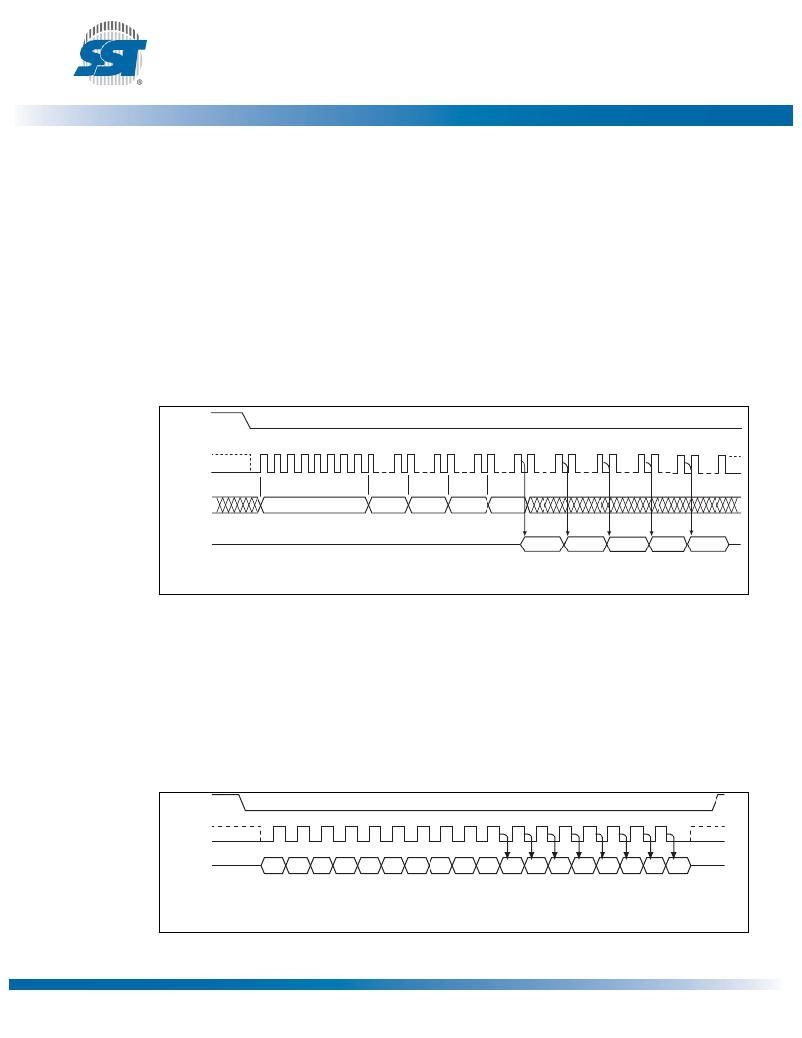
�High-Speed� Read� (80� MHz)�
�The� High-Speed� Read� instruction,� 0BH,� is� supported� in� both� SPI� bus� protocol� and� SQI� protocol.� On�
�power-up,� the� device� is� set� to� use� SPI.�
�Initiate� High-Speed� Read� by� executing� an� 8-bit� command,� 0BH,� followed� by� address� bits� [A23-A0]� and�
�a� dummy� byte.� CE#� must� remain� active� low� for� the� duration� of� the� High-Speed� Read� cycle.� SIO2� and�
�SIO3� must� be� driven� V� IH� for� the� duration� of� the� Read� cycle.� See� Figure� 10� for� the� High-Speed� Read�
�sequence� for� SPI� bus� protocol.�
�CE#�
�MODE� 3�
�0� 1� 2� 3� 4� 5� 6� 7� 8�
�15� 16�
�23� 24�
�31� 32�
�39� 40�
�47� 48�
�55� 56�
�63� 64�
�71� 72�
�80�
�SCK� MODE� 0�
�SI/SIO0�
�0B�
�ADD.�
�ADD.�
�ADD.�
�X�
�SO/SIO1�
�HIGH� IMPEDANCE�
�N�
�D� OUT�
�N+1�
�D� OUT�
�N+2�
�D� OUT�
�N+3�
�D� OUT�
�N+4�
�D� OUT�
�MSB�
�1359� F31.0�
�Note:� SIO2� and� SIO3� must� be� driven� V� IH�
�Figure� 10:� High-Speed� Read� Sequence� (SPI)�
�In� SQI� protocol,� the� host� drives� CE#� low� then� send� the� Read� command� cycle� command,� 0BH,� followed� by�
�three� address� cycles� and� one� dummy� cycle.� Each� cycle� is� two� nibbles� (clocks)� long,� most� significant� nibble� first.�
�After� the� dummy� cycle,� the� Serial� Quad� I/O� (SQI)� Flash� Memory� outputs� data� on� the� falling� edge� of�
�the� SCK� signal� starting� from� the� specified� address� location.� The� device� continually� streams� data� out-�
�put� through� all� addresses� until� terminated� by� a� low-to-high� transition� on� CE#.� The� internal� address�
�pointer� automatically� increments� until� the� highest� memory� address� is� reached,� at� which� point� the�
�address� pointer� returns� to� address� location� 000000H.�
�During� this� operation,� blocks� that� are� Read-locked� will� output� data� 00H.�
�CE#�
�MODE� 3�
�0�
�1�
�2�
�9�
�16�
�MODE� 3�
�CLK�
�MODE� 0�
�MODE� 0�
�SIO(3:0)�
�C1� C0�
�A5�
�A4�
�A3�
�A2�
�A1�
�A0�
�X�
�X�
�H0�
�L0�
�H1�
�L1�
�H2�
�L2�
�H3�
�L3�
�MSB�
�Data� In�
�Note:� C[1:0]� =� 0BH�
�Figure� 11:� High-Speed� Read� Sequence� (SQI)�
�?2011� Silicon� Storage� Technology,� Inc.�
�15�
�Data� Out�
�DS-25017A�
�1359� F06.2�
�04/11�
�相关PDF资料 |
PDF描述 |
|---|---|
| SST39LF200A-55-4C-B3KE-T | IC FLASH MPF 2MBIT 55NS 48TFBGA |
| XC6SLX150T-3FG676I | IC FPGA SPARTAN 6 676FGGBGA |
| XCV200E-7FG256I | IC FPGA 1.8V I-TEMP 256-FBGA |
| SST39SF020A-45-4C-WHE | IC FLASH MPF 2MBIT 45NS 32TSOP |
| SST39SF020A-70-4I-WHE | IC FLASH MPF 2MBIT 70NS 32TSOP |
相关代理商/技术参数 |
参数描述 |
|---|---|
| SST26VF016-80-5I-QAE-T | 功能描述:闪存 2.7 to 3.6V 16Mbit Serial Quad I/O Flsh RoHS:否 制造商:ON Semiconductor 数据总线宽度:1 bit 存储类型:Flash 存储容量:2 MB 结构:256 K x 8 定时类型: 接口类型:SPI 访问时间: 电源电压-最大:3.6 V 电源电压-最小:2.3 V 最大工作电流:15 mA 工作温度:- 40 C to + 85 C 安装风格:SMD/SMT 封装 / 箱体: 封装:Reel |
| SST26VF016-80-5I-QE | 制造商:SST 制造商全称:Silicon Storage Technology, Inc 功能描述:Serial Quad I/O (SQI) Flash Memory |
| SST26VF016-80-5I-S2AE | 功能描述:闪存 16M 80MHz 2.7-3.6V Industrial RoHS:否 制造商:ON Semiconductor 数据总线宽度:1 bit 存储类型:Flash 存储容量:2 MB 结构:256 K x 8 定时类型: 接口类型:SPI 访问时间: 电源电压-最大:3.6 V 电源电压-最小:2.3 V 最大工作电流:15 mA 工作温度:- 40 C to + 85 C 安装风格:SMD/SMT 封装 / 箱体: 封装:Reel |
| SST26VF016-80-5I-S2AE-T | 功能描述:闪存 2.7 to 3.6V 16Mbit Serial Quad I/O Flsh RoHS:否 制造商:ON Semiconductor 数据总线宽度:1 bit 存储类型:Flash 存储容量:2 MB 结构:256 K x 8 定时类型: 接口类型:SPI 访问时间: 电源电压-最大:3.6 V 电源电压-最小:2.3 V 最大工作电流:15 mA 工作温度:- 40 C to + 85 C 安装风格:SMD/SMT 封装 / 箱体: 封装:Reel |
| SST26VF016-80-5I-S2E | 制造商:SST 制造商全称:Silicon Storage Technology, Inc 功能描述:Serial Quad I/O (SQI) Flash Memory |
发布紧急采购,3分钟左右您将得到回复。