- 您现在的位置:买卖IC网 > PDF目录4236 > SST26VF016-80-5I-QAE (Microchip Technology)IC FLASH SER 16M 80MHZ SQI 8WSON PDF资料下载
参数资料
| 型号: | SST26VF016-80-5I-QAE |
| 厂商: | Microchip Technology |
| 文件页数: | 21/39页 |
| 文件大小: | 0K |
| 描述: | IC FLASH SER 16M 80MHZ SQI 8WSON |
| 标准包装: | 98 |
| 系列: | SST26 SQI® |
| 格式 - 存储器: | 闪存 |
| 存储器类型: | FLASH |
| 存储容量: | 16M(2M x 8) |
| 速度: | 80MHz |
| 接口: | Serial Quad I/O™(SQI™) |
| 电源电压: | 2.7 V ~ 3.6 V |
| 工作温度: | -40°C ~ 85°C |
| 封装/外壳: | 8-WDFN 裸露焊盘 |
| 供应商设备封装: | 8-WSON |
| 包装: | 管件 |
第1页第2页第3页第4页第5页第6页第7页第8页第9页第10页第11页第12页第13页第14页第15页第16页第17页第18页第19页第20页当前第21页第22页第23页第24页第25页第26页第27页第28页第29页第30页第31页第32页第33页第34页第35页第36页第37页第38页第39页
�� �
�
�Serial� Quad� I/O� (SQI)� Flash� Memory�
�A� Microchip� Technology� Company�
�SST26VF016� /� SST26VF032�
�Data� Sheet�
�Page-Program�
�The� Page-Program� instruction� programs� up� to� 256� Bytes� of� data� in� the� memory.� The� data� for� the�
�selected� page� address� must� be� in� the� erased� state� (FFH)� before� initiating� the� Page-Program� operation.�
�A� Page-Program� applied� to� a� protected� memory� area� will� be� ignored.� Prior� to� the� program� operation,�
�execute� the� WREN� instruction.�
�To� execute� a� Page-Program� operation,� the� host� drives� CE#� low� then� sends� the� Page� Program� com-�
�mand� cycle� (02H),� three� address� cycles� followed� by� the� data� to� be� programmed,� then� drives� CE#� high.�
�The� programmed� data� must� be� between� 1� to� 256� Bytes� and� in� whole� Byte� increments;� sending� an� odd�
�number� of� nibbles� will� cause� the� last� nibble� to� be� ignored.� Each� cycle� is� two� nibbles� (clocks)� long,� most�
�significant� bit� first.� Poll� the� BUSY� bit� in� the� Status� register� or� wait� T� PP� for� the� completion� of� the� internal,�
�self-timed,� Page-Program� operat� i� on.� See� Figure� 18� for� the� Page-Program� sequence.�
�When� executing� Page-Program,� the� memory� range� for� the� SST26VF016/032� is� divided� into� 256� Byte�
�page� boundaries.� The� device� handles� shifting� of� more� than� 256� Bytes� of� data� by� maintaining� the� last�
�256� Bytes� of� data� as� the� correct� data� to� be� programmed.� If� the� target� address� for� the� Page-Program�
�instruction� is� not� the� beginning� of� the� page� boundary� (A7:A0� are� not� all� zero),� and� the� number� of� data�
�input� exceeds� or� overlaps� the� end� of� the� address� of� the� page� boundary,� the� excess� data� inputs� wrap�
�around� and� will� be� programmed� at� the� start� of� that� target� page.�
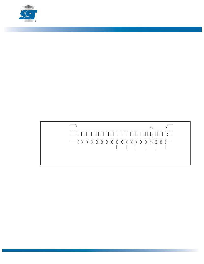
�CE#�
�MODE� 3�
�0�
�2�
�4�
�6�
�8�
�10�
�12�
�542�
�SCK�
�MODE� 0�
�SIO(3:0)�
�C1� C0� A5� A4� A3� A2� A1� A0� H0� L0� H1� L1� H2� L2�
�MSN� LSN�
�Data� Byte� 0� Data� Byte� 1� Data� Byte� 2�
�HN� LN�
�Data� Byte� 255�
�1359� F10.0�
�Note:� MSN� =� Most� Significant� Nibble,� LSN� =� Least� Significant� Nibble�
�C[1:0]� =� 02H�
�Figure� 18:� Page-Program� Sequence�
�Write-Suspend� and� Write-Resume�
�Write-Suspend� allows� the� interruption� of� Sector-Erase,� Block-Erase� or� Page-Program� operations� in�
�order� to� erase,� program,� or� read� data� in� another� portion� of� memory.� The� original� operation� can� be� con-�
�tinued� with� the� Write-Resume� command.�
�Only� one� write� operation� can� be� suspended� at� a� time;� if� an� operation� is� already� suspended,� the� device�
�will� ignore� the� Write-Suspend� command.� Write-Suspend� during� Chip-Erase� is� ignored;� Chip-Erase� is�
�not� a� valid� command� while� a� write� is� suspended.�
�?2011� Silicon� Storage� Technology,� Inc.�
�21�
�DS-25017A�
�04/11�
�相关PDF资料 |
PDF描述 |
|---|---|
| SST39LF200A-55-4C-B3KE-T | IC FLASH MPF 2MBIT 55NS 48TFBGA |
| XC6SLX150T-3FG676I | IC FPGA SPARTAN 6 676FGGBGA |
| XCV200E-7FG256I | IC FPGA 1.8V I-TEMP 256-FBGA |
| SST39SF020A-45-4C-WHE | IC FLASH MPF 2MBIT 45NS 32TSOP |
| SST39SF020A-70-4I-WHE | IC FLASH MPF 2MBIT 70NS 32TSOP |
相关代理商/技术参数 |
参数描述 |
|---|---|
| SST26VF016-80-5I-QAE-T | 功能描述:闪存 2.7 to 3.6V 16Mbit Serial Quad I/O Flsh RoHS:否 制造商:ON Semiconductor 数据总线宽度:1 bit 存储类型:Flash 存储容量:2 MB 结构:256 K x 8 定时类型: 接口类型:SPI 访问时间: 电源电压-最大:3.6 V 电源电压-最小:2.3 V 最大工作电流:15 mA 工作温度:- 40 C to + 85 C 安装风格:SMD/SMT 封装 / 箱体: 封装:Reel |
| SST26VF016-80-5I-QE | 制造商:SST 制造商全称:Silicon Storage Technology, Inc 功能描述:Serial Quad I/O (SQI) Flash Memory |
| SST26VF016-80-5I-S2AE | 功能描述:闪存 16M 80MHz 2.7-3.6V Industrial RoHS:否 制造商:ON Semiconductor 数据总线宽度:1 bit 存储类型:Flash 存储容量:2 MB 结构:256 K x 8 定时类型: 接口类型:SPI 访问时间: 电源电压-最大:3.6 V 电源电压-最小:2.3 V 最大工作电流:15 mA 工作温度:- 40 C to + 85 C 安装风格:SMD/SMT 封装 / 箱体: 封装:Reel |
| SST26VF016-80-5I-S2AE-T | 功能描述:闪存 2.7 to 3.6V 16Mbit Serial Quad I/O Flsh RoHS:否 制造商:ON Semiconductor 数据总线宽度:1 bit 存储类型:Flash 存储容量:2 MB 结构:256 K x 8 定时类型: 接口类型:SPI 访问时间: 电源电压-最大:3.6 V 电源电压-最小:2.3 V 最大工作电流:15 mA 工作温度:- 40 C to + 85 C 安装风格:SMD/SMT 封装 / 箱体: 封装:Reel |
| SST26VF016-80-5I-S2E | 制造商:SST 制造商全称:Silicon Storage Technology, Inc 功能描述:Serial Quad I/O (SQI) Flash Memory |
发布紧急采购,3分钟左右您将得到回复。