- 您现在的位置:买卖IC网 > PDF目录195454 > SST49LF003B-33-4C-NH (SILICON STORAGE TECHNOLOGY INC) 384K X 8 FLASH 3V PROM, 11 ns, PQCC32 PDF资料下载
参数资料
| 型号: | SST49LF003B-33-4C-NH |
| 厂商: | SILICON STORAGE TECHNOLOGY INC |
| 元件分类: | PROM |
| 英文描述: | 384K X 8 FLASH 3V PROM, 11 ns, PQCC32 |
| 封装: | PLASTIC, MS-016AE, LCC-32 |
| 文件页数: | 11/43页 |
| 文件大小: | 500K |
| 代理商: | SST49LF003B-33-4C-NH |
第1页第2页第3页第4页第5页第6页第7页第8页第9页第10页当前第11页第12页第13页第14页第15页第16页第17页第18页第19页第20页第21页第22页第23页第24页第25页第26页第27页第28页第29页第30页第31页第32页第33页第34页第35页第36页第37页第38页第39页第40页第41页第42页第43页
Data Sheet
2 Mbit / 3 Mbit / 4 Mbit LPC Firmware Flash
SST49LF002B / SST49LF003B / SST49LF004B
19
2005 Silicon Storage Technology, Inc.
S71232-05-000
1/05
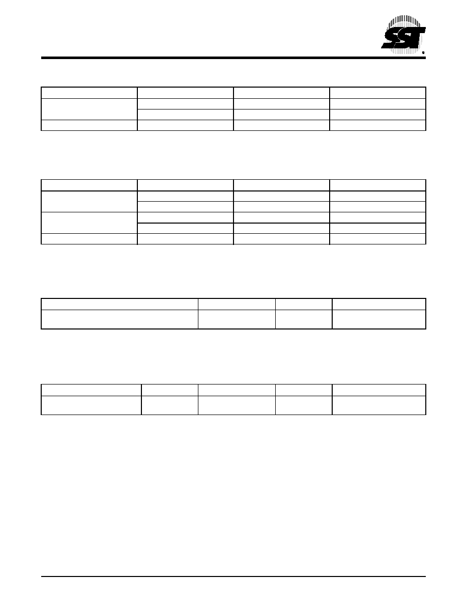
TABLE
9: LPC MEMORY ADDRESS DECODING RANGE FOR SST49LF002B
ID Strapping
Device Access
Address Range
Memory Size
Device #0 - 15
Memory Access
FFFF FFFFH : FFC0 0000H
4 MByte
Register Access
FFBF FFFFH : FF80 0000H
4 MByte
Device #01
Memory Access
000F FFFFH : 000E 0000H
128 KByte
T9.1 1232
1. For device #0 (Boot Device), SST49LF002B decodes the physical addresses of the top 8 blocks (including Boot Block) both at sys-
tem memory ranges FFFF FFFFH to FFFE 0000H and 000F FFFFH to 000E 0000H.
TABLE 10: LPC MEMORY ADDRESS DECODING RANGE FOR SST49LF003B1 AND SST49LF004B
1. For the SST49LF003B, operations beyond the 3 Mbit boundary (below 20000H) are not valid (see Device Memory Map).
ID Strapping
Device Access
Address Range
Memory Size
Device #0 - 7
Memory Access
FFFF FFFFH : FFC0 0000H
4 MByte
Register Access
FFBF FFFFH : FF80 0000H
4 MByte
Device #8 - 15
Memory Access
FF7F FFFFH : FF40 0000H
4 MByte
Register Access
FF3F FFFFH : FF00 0000H
4 MByte
Device #02
2. For device #0 (Boot Device), SST49LF003B/004B decodes the physical addresses of the top 2 blocks (including Boot Block) both at
system memory ranges FFFF FFFFH to FFFE 0000H and 000F FFFFH to 000E 0000H.
Memory Access
000F FFFFH : 000E 0000H
128 KByte
T10.0 1232
TABLE 11: SST49LF002B LPC MEMORY ADDRESS BITS DEFINITION
A31: A231
1. For SST49LF002B, the top 8 MByte address range FFFF FFFFH to FF80 0000H and the bottom 128 KByte memory access address
000F FFFFH to 000E 0000H are decoded.
A22
A21: A18
A17:A0
1111 1111b or 0000 0000b
1 = Memory Access
0 = Register access
ID[3:0]2
2. See Table 14 for multiple device selection configuration.
Device Memory address
T11.0 1232
TABLE 12: SST49LF003B1 AND SST49LF004B LPC MEMORY ADDRESS BITS DEFINITION
1. For the SST49LF003B, operations beyond the 3 Mbit boundary (below 20000H) are not valid (see Device Memory Map).
A31: A242
2. For SST49LF003B/004B, the top 16 MByte address range FFFF FFFFH to FF00 0000H and the bottom 128 KByte memory access
address 000F FFFFH to 000E 0000H are decoded.
A23
A22
A21: A19
A18:A0
1111 1111b or 0000 0000b
ID[3]3
3. See Table 14 for multiple device selection configuration.
1 = Memory Access
0 = Register access
Device Memory address
T12.0 1232
相关PDF资料 |
PDF描述 |
|---|---|
| SSTAR-01 | SPECIALTY TELECOM CIRCUIT |
| SSTV16857MTDX | |
| SSTV16857MTDX_NL | |
| SSTV16857MTD_NL | |
| SSW-1-05-22-SM-S-VS | 5 CONTACT(S), FEMALE, STRAIGHT TWO PART BOARD CONNECTOR, SURFACE MOUNT |
相关代理商/技术参数 |
参数描述 |
|---|---|
| SST49LF004A | 制造商:SST 制造商全称:Silicon Storage Technology, Inc 功能描述:2 Mbit / 3 Mbit / 4 Mbit / 8 Mbit Firmware Hub |
| SST49LF004A-33-4C-NH | 制造商:Silicon Storage Technology (SST) 功能描述:NOR Flash, 512K x 8, 32 Pin, Plastic, PLCC |
| SST49LF004A-33-4C-WH | 制造商:SST 制造商全称:Silicon Storage Technology, Inc 功能描述:2 Mbit / 3 Mbit / 4 Mbit / 8 Mbit Firmware Hub |
| SST49LF004B | 制造商:SST 制造商全称:Silicon Storage Technology, Inc 功能描述:4 Mbit Firmware Hub |
| SST49LF004B_06 | 制造商:SST 制造商全称:Silicon Storage Technology, Inc 功能描述:4 Mbit Firmware Hub |
发布紧急采购,3分钟左右您将得到回复。