- 您现在的位置:买卖IC网 > PDF目录195454 > SST49LF003B-33-4C-NH (SILICON STORAGE TECHNOLOGY INC) 384K X 8 FLASH 3V PROM, 11 ns, PQCC32 PDF资料下载
参数资料
| 型号: | SST49LF003B-33-4C-NH |
| 厂商: | SILICON STORAGE TECHNOLOGY INC |
| 元件分类: | PROM |
| 英文描述: | 384K X 8 FLASH 3V PROM, 11 ns, PQCC32 |
| 封装: | PLASTIC, MS-016AE, LCC-32 |
| 文件页数: | 13/43页 |
| 文件大小: | 500K |
| 代理商: | SST49LF003B-33-4C-NH |
第1页第2页第3页第4页第5页第6页第7页第8页第9页第10页第11页第12页当前第13页第14页第15页第16页第17页第18页第19页第20页第21页第22页第23页第24页第25页第26页第27页第28页第29页第30页第31页第32页第33页第34页第35页第36页第37页第38页第39页第40页第41页第42页第43页
20
Data Sheet
2 Mbit / 3 Mbit / 4 Mbit LPC Firmware Flash
SST49LF002B / SST49LF003B / SST49LF004B
2005 Silicon Storage Technology, Inc.
S71232-05-000
1/05
Multiple Device Selection
Multiple LPC flash devices may be strapped to increase
memory densities in a system. The four ID pins, ID[3:0],
allow up to 16 devices to be attached to the same bus by
using different ID strapping in a system. BIOS support, bus
loading, or the attaching bridge may limit this number. The
boot device must have an ID of 0000b (determined by
ID[3:0]); subsequent devices use incremental numbering.
Equal density must be used with multiple devices.
Multiple Device Selection for
Firmware Memory Cycle
For Firmware Memory Read/Write cycles, hardware strap-
ping values on ID[3:0] must match the values in IDSEL
field. See Table 13 for multiple device selection configura-
tions. The SST49LF00xB will compare the IDSEL field with
ID[3:0]'s strapping values. If there is a mismatch, the device
will ignore the reminder of the cycle.
Multiple Device Selection for LPC Memory Cycle
For LPC Memory Read/Write cycles, ID information is
included in the address bits of every cycle. The ID bits in
the address field are the inverse of the hardware strapping.
See Table 14 for multiple device selection configurations.
The SST49LF00xB will compare these bits with ID[3:0]’s
strapping values. If there is a mismatch, the device will
ignore the remainder of the cycle.
Write Operation Status Detection
The SST49LF00xB device provides two software means to
detect the completion of a Write (Program or Erase) cycle,
in order to optimize the system Write cycle time. The soft-
ware detection includes two status bits: Data# Polling, D[7],
and Toggle Bit, D[6]. The End-of-Write detection mode is
incorporated into the Firmware Memory and LPC Memory
Read cycles. The actual completion of the nonvolatile write
is asynchronous with the system. Therefore, either a Data#
Polling or Toggle Bit read may be simultaneous with the
completion of the Write cycle. If this occurs, the system
may possibly get an erroneous result, i.e., valid data may
appear to conflict with either D[7] or D[6]. In order to prevent
spurious rejection, if an erroneous result occurs, the soft-
ware routine should include a loop to read the accessed
location an additional two (2) times. If both reads are valid,
then the device has completed the Write cycle, otherwise
the rejection is valid.
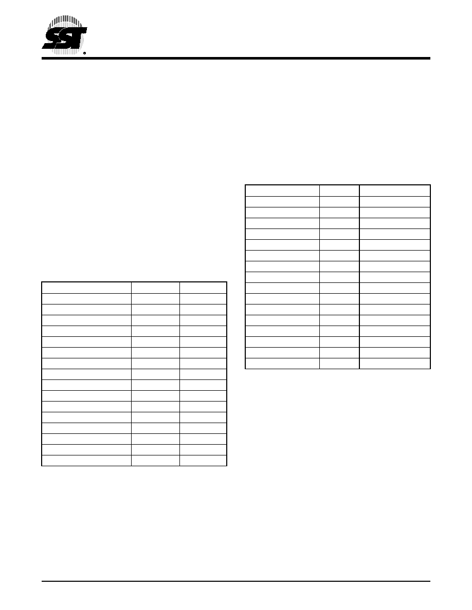
TABLE 13: FIRMWARE MEMORY MULTIPLE DEVICE
SELECTION CONFIGURATION
Device #
ID[3:0]
IDSEL
0 (Boot device)
0000
1
0001
2
0010
3
0011
4
0100
5
0101
6
0110
7
0111
8
1000
9
1001
10
1010
11
1011
12
1100
13
1101
14
1110
15
1111
T13.0 1232
TABLE 14: LPC MEMORY MULTIPLE DEVICE
SELECTION CONFIGURATION
Device #
ID[3:0]
Address Range1
1. For SST49LF002B, A21:A18,
For SST49LF003B/004B, A23, A21:A19
0 (Boot device)
0000
1111
1
0001
1110
2
0010
1101
3
0011
1100
4
0100
1011
5
0101
1010
6
0110
1001
7
0111
1000
8
1000
0111
9
1001
0110
10
1010
0101
11
1011
0100
12
1100
0011
13
1101
0010
14
1110
0001
15
1111
0000
T14.0 1232
相关PDF资料 |
PDF描述 |
|---|---|
| SSTAR-01 | SPECIALTY TELECOM CIRCUIT |
| SSTV16857MTDX | |
| SSTV16857MTDX_NL | |
| SSTV16857MTD_NL | |
| SSW-1-05-22-SM-S-VS | 5 CONTACT(S), FEMALE, STRAIGHT TWO PART BOARD CONNECTOR, SURFACE MOUNT |
相关代理商/技术参数 |
参数描述 |
|---|---|
| SST49LF004A | 制造商:SST 制造商全称:Silicon Storage Technology, Inc 功能描述:2 Mbit / 3 Mbit / 4 Mbit / 8 Mbit Firmware Hub |
| SST49LF004A-33-4C-NH | 制造商:Silicon Storage Technology (SST) 功能描述:NOR Flash, 512K x 8, 32 Pin, Plastic, PLCC |
| SST49LF004A-33-4C-WH | 制造商:SST 制造商全称:Silicon Storage Technology, Inc 功能描述:2 Mbit / 3 Mbit / 4 Mbit / 8 Mbit Firmware Hub |
| SST49LF004B | 制造商:SST 制造商全称:Silicon Storage Technology, Inc 功能描述:4 Mbit Firmware Hub |
| SST49LF004B_06 | 制造商:SST 制造商全称:Silicon Storage Technology, Inc 功能描述:4 Mbit Firmware Hub |
发布紧急采购,3分钟左右您将得到回复。