- 您现在的位置:买卖IC网 > PDF目录195454 > SST49LF003B-33-4C-NH (SILICON STORAGE TECHNOLOGY INC) 384K X 8 FLASH 3V PROM, 11 ns, PQCC32 PDF资料下载
参数资料
| 型号: | SST49LF003B-33-4C-NH |
| 厂商: | SILICON STORAGE TECHNOLOGY INC |
| 元件分类: | PROM |
| 英文描述: | 384K X 8 FLASH 3V PROM, 11 ns, PQCC32 |
| 封装: | PLASTIC, MS-016AE, LCC-32 |
| 文件页数: | 4/43页 |
| 文件大小: | 500K |
| 代理商: | SST49LF003B-33-4C-NH |
第1页第2页第3页当前第4页第5页第6页第7页第8页第9页第10页第11页第12页第13页第14页第15页第16页第17页第18页第19页第20页第21页第22页第23页第24页第25页第26页第27页第28页第29页第30页第31页第32页第33页第34页第35页第36页第37页第38页第39页第40页第41页第42页第43页
12
Data Sheet
2 Mbit / 3 Mbit / 4 Mbit LPC Firmware Flash
SST49LF002B / SST49LF003B / SST49LF004B
2005 Silicon Storage Technology, Inc.
S71232-05-000
1/05
DESIGN CONSIDERATIONS
SST recommends a high frequency 0.1 F ceramic capac-
itor to be placed as close as possible between VDD and
VSS less than 1 cm away from the VDD pin of the device.
Additionally, a low frequency 4.7 F electrolytic capacitor
from VDD to VSS should be placed within 1 cm of the VDD
pin. If a socket is used for programming purposes, an addi-
tional 1-10 F should be added next to each socket.
The RST# and INIT# pins must remain stable at VIH for the
entire duration of an Erase or Program operation. WP#
must remain stable at VIH for the entire duration of the
Erase and Program operations for non-Boot Block sectors.
To write data to the top Boot Block sectors, the TBL# pin
must also remain stable at VIH for the entire duration of the
Erase and Program operations.
PRODUCT IDENTIFICATION
The Product Identification mode identifies the device as the
SST49LF00xB and manufacturer as SST.
MODE SELECTION
The SST49LF00xB flash memory device operates in two
distinct interface modes: the LPC mode and the Parallel
Programming (PP) mode. The MODE (Interface Mode
Select) pin is used to set the interface mode selection. If the
MODE pin is set to logic high, the device is in PP mode;
while if the MODE pin is set low, the device is in LPC mode.
The MODE selection pin must be configured prior to device
operation and must not change during operation. If the pin
is not connected, by default the Mode pin is internally
pulled low and the 49LF00xB will be in LPC operation.
In LPC mode, communication between the Host and the
SST49LF00xB occurs via the 4-bit I/O communication sig-
nals, LAD[3:0] and LFRAME#. The SST49LF00xB detects
whether it is being accessed via a FWH or LPC protocol by
detecting the START field contents; a 1101b or 1110b indi-
cates a Firmware Memory cycle and a 0000b indicates an
LPC memory cycle.
In PP mode, the device is controlled via the 11 addresses,
A10-A0, and 8 I/O, DQ7-DQ0, signals. The address inputs
are multiplexed in row and column selected by control sig-
nal R/C# pin. The row addresses are mapped to the lower
internal addresses (A10-0), and the column addresses are
mapped to the higher internal addresses (AMS-11) shown in
for address assignments.
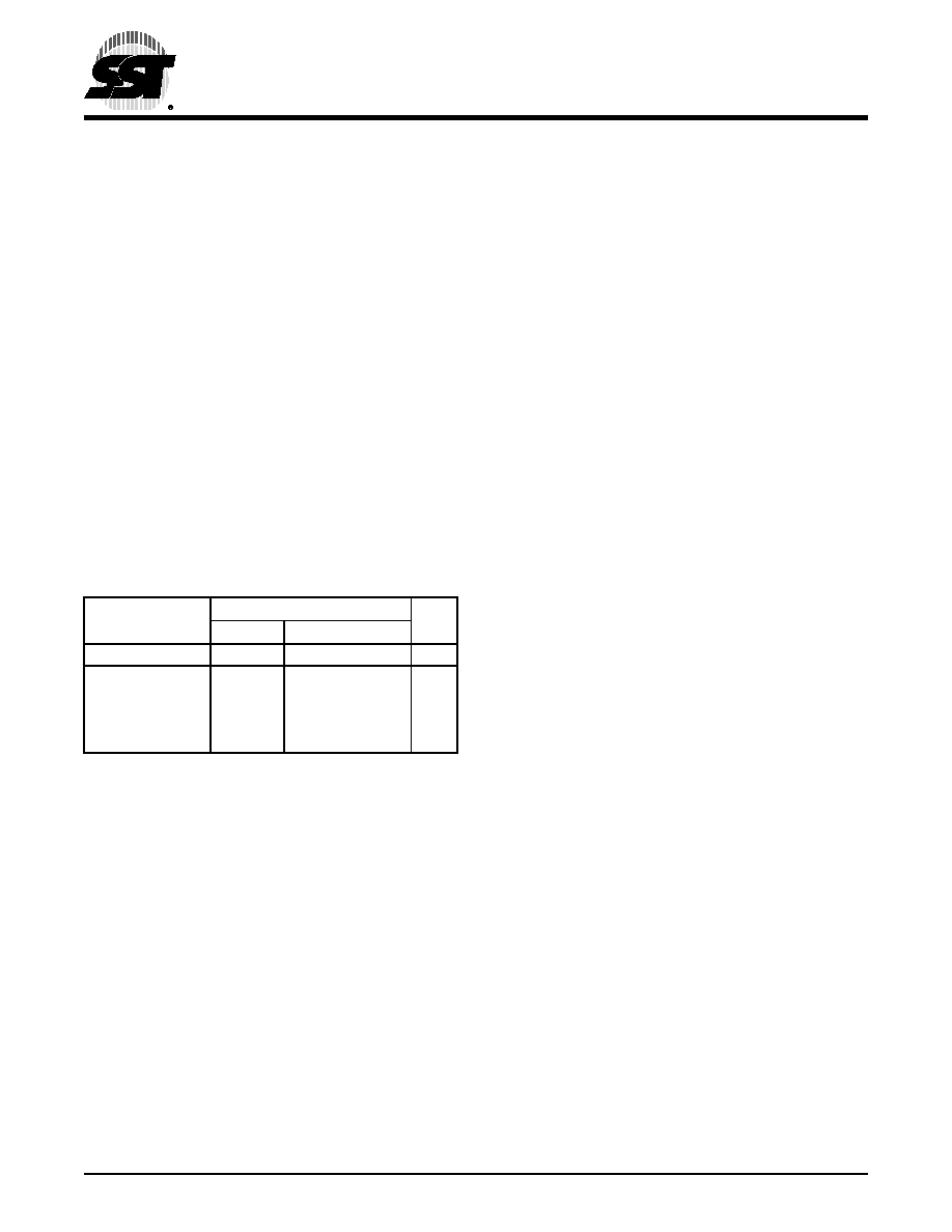
TABLE
3: PRODUCT IDENTIFICATION
Address
Data
PP Mode
LPC Mode1
1. Address shown in this column is for boot device only.
Address locations should appear elsewhere in the 4
GByte system memory map depending on ID strapping
values on ID[3:0] pins when multiple LPC memory
devices are used in a system.
Manufacturer’s ID
0000H
FFBC 0000H
BFH
Device ID2
2. The device ID for SST49LF00xB is the same as
SST49LF00xA.
SST49LF002B
0001H
FFBC 0001H
57H
SST49LF003B
0001H
FFBC 0001H
1BH
SST49LF004B
0001H
FFBC 0001H
60H
T3.1 1232
相关PDF资料 |
PDF描述 |
|---|---|
| SSTAR-01 | SPECIALTY TELECOM CIRCUIT |
| SSTV16857MTDX | |
| SSTV16857MTDX_NL | |
| SSTV16857MTD_NL | |
| SSW-1-05-22-SM-S-VS | 5 CONTACT(S), FEMALE, STRAIGHT TWO PART BOARD CONNECTOR, SURFACE MOUNT |
相关代理商/技术参数 |
参数描述 |
|---|---|
| SST49LF004A | 制造商:SST 制造商全称:Silicon Storage Technology, Inc 功能描述:2 Mbit / 3 Mbit / 4 Mbit / 8 Mbit Firmware Hub |
| SST49LF004A-33-4C-NH | 制造商:Silicon Storage Technology (SST) 功能描述:NOR Flash, 512K x 8, 32 Pin, Plastic, PLCC |
| SST49LF004A-33-4C-WH | 制造商:SST 制造商全称:Silicon Storage Technology, Inc 功能描述:2 Mbit / 3 Mbit / 4 Mbit / 8 Mbit Firmware Hub |
| SST49LF004B | 制造商:SST 制造商全称:Silicon Storage Technology, Inc 功能描述:4 Mbit Firmware Hub |
| SST49LF004B_06 | 制造商:SST 制造商全称:Silicon Storage Technology, Inc 功能描述:4 Mbit Firmware Hub |
发布紧急采购,3分钟左右您将得到回复。