- 您现在的位置:买卖IC网 > PDF目录195454 > SST49LF003B-33-4C-NH (SILICON STORAGE TECHNOLOGY INC) 384K X 8 FLASH 3V PROM, 11 ns, PQCC32 PDF资料下载
参数资料
| 型号: | SST49LF003B-33-4C-NH |
| 厂商: | SILICON STORAGE TECHNOLOGY INC |
| 元件分类: | PROM |
| 英文描述: | 384K X 8 FLASH 3V PROM, 11 ns, PQCC32 |
| 封装: | PLASTIC, MS-016AE, LCC-32 |
| 文件页数: | 9/43页 |
| 文件大小: | 500K |
| 代理商: | SST49LF003B-33-4C-NH |
第1页第2页第3页第4页第5页第6页第7页第8页当前第9页第10页第11页第12页第13页第14页第15页第16页第17页第18页第19页第20页第21页第22页第23页第24页第25页第26页第27页第28页第29页第30页第31页第32页第33页第34页第35页第36页第37页第38页第39页第40页第41页第42页第43页
Data Sheet
2 Mbit / 3 Mbit / 4 Mbit LPC Firmware Flash
SST49LF002B / SST49LF003B / SST49LF004B
17
2005 Silicon Storage Technology, Inc.
S71232-05-000
1/05
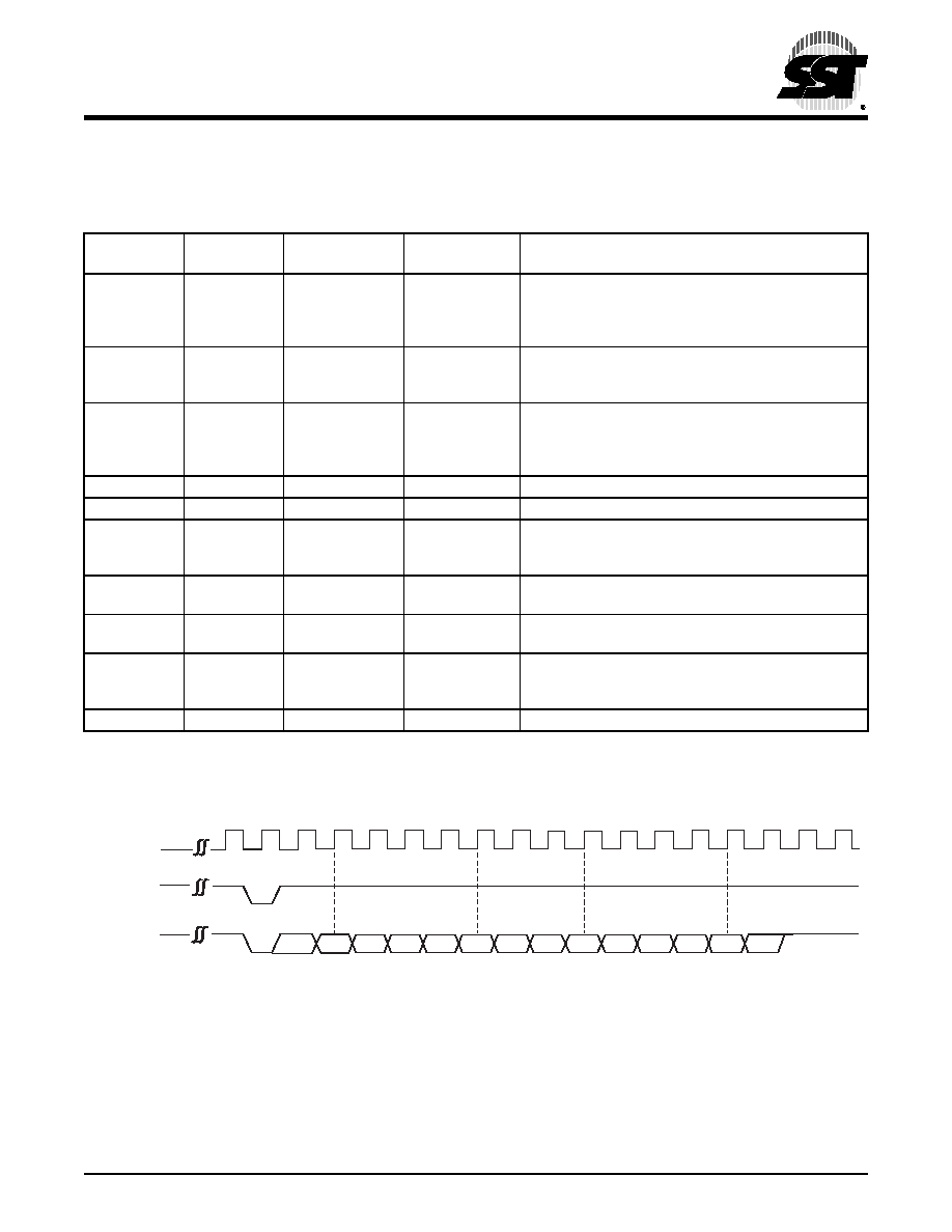
LPC Memory Write Cycle
FIGURE 9: LPC MEMORY WRITE CYCLE WAVEFORM
TABLE
8: LPC MEMORY WRITE CYCLE FIELD DEFINITIONS
Clock
Cycle
Field
Name
Field Contents
LAD[3:0]1
1. Field contents are valid on the rising edge of the present clock cycle.
LAD[3:0]
Direction
Comments
1
START
0000
IN
LFRAME# must be active (low) for the device to
respond. Only the last field latched before LFRAME#
transitions high will be recognized. The START field
contents (0000b) indicate an LPC Memory cycle.
2
CYCTYPE +
DIR
011X
IN
Indicates the type of LPC Memory cycle. Bits 3:2
must be “01b” for memory cycle. Bit 1 indicates the
type of transfer “1” for Write. Bit 0 is reserved.
3-10
ADDR
YYYY
IN
Address Phase for Memory Cycle. LPC protocol sup-
ports a 32-bit address phase. YYYY is one nibble of
the entire address. Addresses are transferred most
significant nibble first.
11
DATA
ZZZZ
IN
ZZZZ is the least-significant nibble of the data byte.
12
DATA
ZZZZ
IN
ZZZZ is the most-significant nibble of the data byte.
13
TAR0
1111
IN
In this clock cycle, the host drives the bus to all '1's and
then floats the bus. This is the first part of the bus “turn-
around cycle.”
14
TAR1
1111 (float)
Float then OUT
The SST49LF00xB takes control of the bus during this
cycle.
15
SYNC
0000
OUT
The SST49LF00xB outputs the values 0000, indicating
that it has received data or a flash command.
16
TAR0
1111
OUT then Float
In this clock cycle, the SST49LF00xB drives the bus to
all '1's and then floats the bus. This is the first part of
the bus “turnaround cycle.”
17
TAR1
1111 (float)
Float then IN
Host resumes control of the bus during this cycle.
T8.0 1232
1232 F06.1
LFRAME#
LAD[3:0]
0000b
011Xb
A[23:20] A[19:16]
A[3:0]
A[7:4]
A[11:8]
A[15:12]
1111b
Tri-State
2 Clocks
TAR0
Load Address in 8 Clocks
Address
1 Clock
Start
CYCTYPE
+
DIR
TAR
1 Clock
Sync
Data
Load Data in 2 Clocks
0000b
D[7:4]
D[3:0]
LCLK
A[31:28] A[27:24]
Data
TAR1
相关PDF资料 |
PDF描述 |
|---|---|
| SSTAR-01 | SPECIALTY TELECOM CIRCUIT |
| SSTV16857MTDX | |
| SSTV16857MTDX_NL | |
| SSTV16857MTD_NL | |
| SSW-1-05-22-SM-S-VS | 5 CONTACT(S), FEMALE, STRAIGHT TWO PART BOARD CONNECTOR, SURFACE MOUNT |
相关代理商/技术参数 |
参数描述 |
|---|---|
| SST49LF004A | 制造商:SST 制造商全称:Silicon Storage Technology, Inc 功能描述:2 Mbit / 3 Mbit / 4 Mbit / 8 Mbit Firmware Hub |
| SST49LF004A-33-4C-NH | 制造商:Silicon Storage Technology (SST) 功能描述:NOR Flash, 512K x 8, 32 Pin, Plastic, PLCC |
| SST49LF004A-33-4C-WH | 制造商:SST 制造商全称:Silicon Storage Technology, Inc 功能描述:2 Mbit / 3 Mbit / 4 Mbit / 8 Mbit Firmware Hub |
| SST49LF004B | 制造商:SST 制造商全称:Silicon Storage Technology, Inc 功能描述:4 Mbit Firmware Hub |
| SST49LF004B_06 | 制造商:SST 制造商全称:Silicon Storage Technology, Inc 功能描述:4 Mbit Firmware Hub |
发布紧急采购,3分钟左右您将得到回复。