- 您现在的位置:买卖IC网 > PDF目录98142 > SST55LC100M-45-C-BWE IDE COMPATIBLE, FLASH MEMORY DRIVE CONTROLLER, PBGA84 PDF资料下载
参数资料
| 型号: | SST55LC100M-45-C-BWE |
| 元件分类: | 存储控制器/管理单元 |
| 英文描述: | IDE COMPATIBLE, FLASH MEMORY DRIVE CONTROLLER, PBGA84 |
| 封装: | 9 X 9 MM, ROHS COMPLIANT, TFBGA-84 |
| 文件页数: | 2/75页 |
| 文件大小: | 1040K |
| 代理商: | SST55LC100M-45-C-BWE |
第1页当前第2页第3页第4页第5页第6页第7页第8页第9页第10页第11页第12页第13页第14页第15页第16页第17页第18页第19页第20页第21页第22页第23页第24页第25页第26页第27页第28页第29页第30页第31页第32页第33页第34页第35页第36页第37页第38页第39页第40页第41页第42页第43页第44页第45页第46页第47页第48页第49页第50页第51页第52页第53页第54页第55页第56页第57页第58页第59页第60页第61页第62页第63页第64页第65页第66页第67页第68页第69页第70页第71页第72页第73页第74页第75页
10
Advance Information
CompactFlash Card Controller
SST55LC100M
2006 Silicon Storage Technology, Inc.
S71316-00-000
3/06
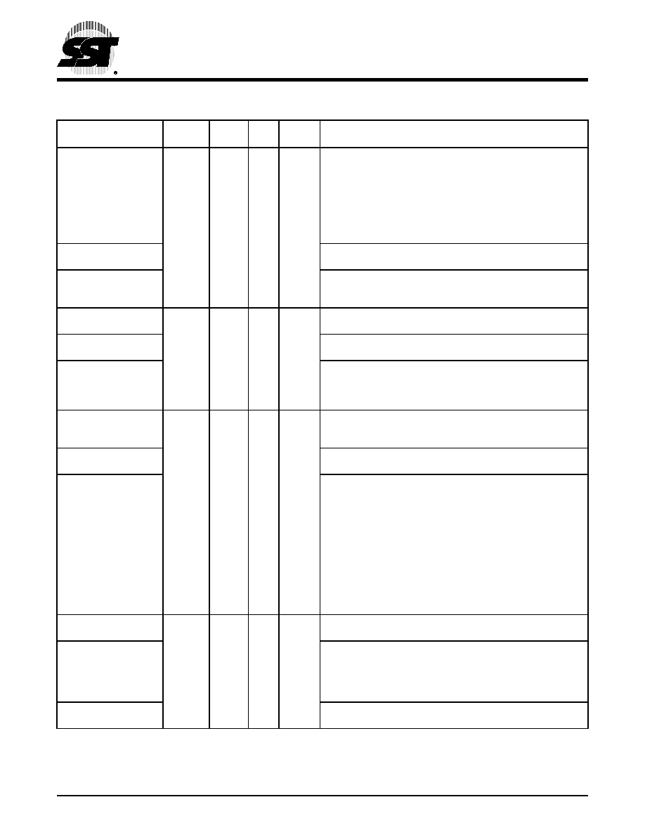
CE1#, CE2#
(Memory Card mode)
24
52
H2
K9
II3U
Card Enable: These input signals are used both to select the
card and to indicate to the card whether a byte or a word oper-
ation is being performed. CE2# always accesses the Odd Byte
of the word. CE1# accesses the Even Byte or the Odd Byte of
the word depending on A0 and CE2#. A multiplexing scheme
based on A0, CE1#, CE2# allows 8-bit hosts to access all data
on D0-D7.
CE1#, CE2#
(PC Card I/O mode)
Card Enable: This signal is the same as the PC Card Memory
mode signal.
CS0#, CS1#
(True IDE mode)
In the True IDE mode CS0# is the chip select for the task file
registers while CS1# is used to select the Alternate Status reg-
ister and the Device Control register.
CSEL#
(Memory Card mode)
56
J10
I
I2U
This signal is not used for this mode.
CSEL#
(PC Card I/O mode)
This signal is not used for this mode.
CSEL#
(True IDE mode)
This internally pulled up signal is used to configure this device
as a master or a slave when configured in the True IDE mode.
When this pin is grounded, this device is configured as a mas-
ter. When the pin is open, this device is configured as a slave.
D15-D0
(Memory Card mode)
65
66
67
68
70
71
72
73
3
4
5
6
8
9
10
11
F8
E10
E9
E8
D10
D9
C10
D8
C3
C4
B2
D4
C2
D3
C1
D2
I/O
I2D, O2
These lines carry the Data, Commands and Status information
between the host and the controller. D0 is the LSB of the Even
Byte of the Word. D8 is the LSB of the Odd Byte of the Word.
D15-D0
(PC Card I/O mode)
This signal is the same as the PC Card Memory mode signal.
D15-D0
(True IDE mode)
In True IDE mode, all Task File operations occur in Byte-Mode
on the low order bus D7-D0 while all data transfers are 16 bit
using D15-D0.
INPACK#
(Memory Card mode)
14
E3
O
O1
This signal is not used in this mode.
INPACK#
(PC Card I/O mode)
The Input Acknowledge signal is asserted by the Compact-
Flash card when the card is selected and responding to an I/O
read cycle at the address that is on the address bus. This sig-
nal is used by the host to control the enable of any input data
buffers between the CompactFlash card and the CPU.
Reserved
(True IDE mode)
In True IDE mode this output signal is not used and should not
be connected at the host.
TABLE
3-1:Pin Assignments (Continued) (2 of 6)
Signal Name
100-lead 84-ball
Pin
Type
I/O
Type1
Name and Functions
相关PDF资料 |
PDF描述 |
|---|---|
| SST55LD017D-40-C-TQWE | FLASH MEMORY DRIVE CONTROLLER, PQFP100 |
| SST55LD017D-40-I-TQW | FLASH MEMORY DRIVE CONTROLLER, PQFP100 |
| SST55LD019A-45-C-TQPE | FLASH MEMORY DRIVE CONTROLLER, PQFP64 |
| SST55LD019C-45-I-BWE | FLASH MEMORY DRIVE CONTROLLER, PBGA84 |
| SST55LD019B-45-C-TQW | FLASH MEMORY DRIVE CONTROLLER, PQFP100 |
相关代理商/技术参数 |
参数描述 |
|---|---|
| SST55LC100M-45-C-TQWE | 功能描述:总线收发器 Compact Flash 45MHz 3.3V Commercial RoHS:否 制造商:Fairchild Semiconductor 逻辑类型:CMOS 逻辑系列:74VCX 每芯片的通道数量:16 输入电平:CMOS 输出电平:CMOS 输出类型:3-State 高电平输出电流:- 24 mA 低电平输出电流:24 mA 传播延迟时间:6.2 ns 电源电压-最大:2.7 V, 3.6 V 电源电压-最小:1.65 V, 2.3 V 最大工作温度:+ 85 C 封装 / 箱体:TSSOP-48 封装:Reel |
| SST55LC100M-45-I-BWE | 制造商:SST 制造商全称:Silicon Storage Technology, Inc 功能描述:CompactFlash Card Controller |
| SST55LC100M-45-I-TQWE | 制造商:SST 制造商全称:Silicon Storage Technology, Inc 功能描述:CompactFlash Card Controller |
| SST55LC200-60-C-TQWE | 功能描述:闪存 Compact 闪存 60MHz 3.3V Commercial RoHS:否 制造商:ON Semiconductor 数据总线宽度:1 bit 存储类型:Flash 存储容量:2 MB 结构:256 K x 8 定时类型: 接口类型:SPI 访问时间: 电源电压-最大:3.6 V 电源电压-最小:2.3 V 最大工作电流:15 mA 工作温度:- 40 C to + 85 C 安装风格:SMD/SMT 封装 / 箱体: 封装:Reel |
| SST55LC200-60-I-TQWE | 功能描述:闪存 Compact 闪存 60MHz 3.3V Commercial RoHS:否 制造商:ON Semiconductor 数据总线宽度:1 bit 存储类型:Flash 存储容量:2 MB 结构:256 K x 8 定时类型: 接口类型:SPI 访问时间: 电源电压-最大:3.6 V 电源电压-最小:2.3 V 最大工作电流:15 mA 工作温度:- 40 C to + 85 C 安装风格:SMD/SMT 封装 / 箱体: 封装:Reel |
发布紧急采购,3分钟左右您将得到回复。