- 您现在的位置:买卖IC网 > PDF目录98143 > ST10F168-Q2 (STMICROELECTRONICS) 16-BIT, FLASH, 25 MHz, MICROCONTROLLER, PQFP144 PDF资料下载
参数资料
| 型号: | ST10F168-Q2 |
| 厂商: | STMICROELECTRONICS |
| 元件分类: | 微控制器/微处理器 |
| 英文描述: | 16-BIT, FLASH, 25 MHz, MICROCONTROLLER, PQFP144 |
| 封装: | 28 X 28 MM, PLASTIC, QFP-144 |
| 文件页数: | 50/76页 |
| 文件大小: | 483K |
| 代理商: | ST10F168-Q2 |
第1页第2页第3页第4页第5页第6页第7页第8页第9页第10页第11页第12页第13页第14页第15页第16页第17页第18页第19页第20页第21页第22页第23页第24页第25页第26页第27页第28页第29页第30页第31页第32页第33页第34页第35页第36页第37页第38页第39页第40页第41页第42页第43页第44页第45页第46页第47页第48页第49页当前第50页第51页第52页第53页第54页第55页第56页第57页第58页第59页第60页第61页第62页第63页第64页第65页第66页第67页第68页第69页第70页第71页第72页第73页第74页第75页第76页
ST10F168
54/76
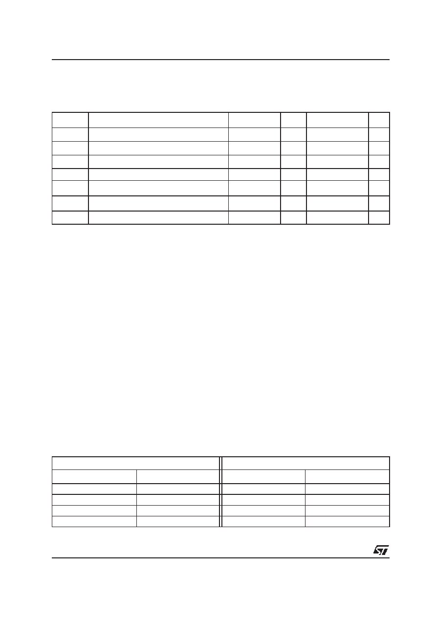
20.4 - A/D Converter Characteristics
VDD =5V ±10%, VSS = 0V, 4.0V ≤ VAREF ≤ VDD + 0.1V, VSS - 0.1V ≤ VAGND ≤ VSS + 0.2V, Q6 version :
TA = -40, +85°C and for Q2 version TA = -40°C, +125°C, unless otherwise specified
Notes 1. VAIN may exceed VAGND or VAREF up to the absolute maximum ratings. However, the conversion result in these cases will be
X000H or X3FFH, respectively.
2. Sample and conversion time are programmable, use table below to calculate values.
3. During the sample time the input capacitance CI can be charged / discharged by the external source. The internal resistance of the
analog source must allow the capacitance to reach its final voltage level within tS. After the end of the sample time tS, changes of the
analog input voltage have no effect on the conversion result.
Values for the sample clock tSC depend on programming and can be taken from the table below.
4. This parameter is fixed by ADC control logic.
5. This parameter includes the sample time tS, the time for determining the digital result and the time to load the result register with
the conversion result.
Values for the conversion clock tCC depend on programming and can be taken from the table below.
6. TUE is tested at VAREF = 5.0V, VAGND = 0V, VCC = 4.9V. It is guaranteed by design characterization for all other voltages within the
defined voltage range.
The specified TUE is guaranteed only if an overload condition (see IOV specification) occurs on maximum of 2 not selected analog
input pins and the absolute sum of input overload currents on all analog input pins does not exceed 10mA.
During the reset calibration sequence the maximum TUE may be
±4 LSB.
7. During the conversion the ADC’s capacitance must be repeatedly charged or discharged. The internal resistance of the reference
voltage source must allow the capacitance to reach its respective voltage level within tCC. The maximum internal resistance results
from the programmed conversion timing.
8. Partially tested, guaranteed by design characterization.
ADC Sample time and conversion time are programmable. The table below should be used to calculate
the above timings.
Symbol
Parameter
Test Conditions
Min.
Max.
Unit
VAIN
SR Analog input voltage range
1
VAGND
VAREF
V
tS
CC Sample time2
34
–
2tSC
tC
CC Conversion time2
54
–
14 tCC +tCS + 4TCL
TUE
CC Total unadjusted error
6
–
± 2
LSB
RAREF SR Internal resistance of reference voltage source
tCC in [ns]
78
–
tCC / 165 - 0.25
k
RASRC SR Internal resistance of analog source
tS in [ns]
38
–
tS / 330 - 0.25
k
CAIN CC ADC input capacitance
8
–
33
pF
Conversion Time
Sample Time
ADCON.15|14 (ADCTC)
Conversion clock tCC
ADCON.13|12 (ADSTC)
Sample clock tSC
00
TCL x 24
00
tCC
01
Reserved, do not use
01
tCC x2
10
TCL x 96
10
tCC x4
11
TCL x 48
11
tCC x8
相关PDF资料 |
PDF描述 |
|---|---|
| ST10F168-Q3 | 16-BIT, FLASH, 25 MHz, MICROCONTROLLER, PQFP144 |
| ST10F252M-4T3 | 16-BIT, FLASH, 40 MHz, RISC MICROCONTROLLER, PQFP100 |
| ST10F269DIETR | 16-BIT, FLASH, 32 MHz, MICROCONTROLLER, UUC |
| ST10F269Z2Q3 | 16-BIT, FLASH, 40 MHz, MICROCONTROLLER, PQFP144 |
| ST10F269Z2Q6 | 16-BIT, FLASH, 40 MHz, MICROCONTROLLER, PQFP144 |
相关代理商/技术参数 |
参数描述 |
|---|---|
| ST10F168Q3 | 制造商:STMicroelectronics 功能描述:MicroController, 16-Bit, 144 Pin, Plastic, QFP |
| ST10F168-Q3 | 制造商:STMicroelectronics 功能描述:MicroController, 16-Bit, 144 Pin, Plastic, QFP |
| ST10F168-Q6 | 制造商:STMICROELECTRONICS 制造商全称:STMicroelectronics 功能描述:16-BIT MCU WITH 256K BYTE FLASH MEMORY AND 8K BYTE RAM |
| ST10F168SQ3 | 功能描述:16位微控制器 - MCU 256K Flash 8K RAM RoHS:否 制造商:Texas Instruments 核心:RISC 处理器系列:MSP430FR572x 数据总线宽度:16 bit 最大时钟频率:24 MHz 程序存储器大小:8 KB 数据 RAM 大小:1 KB 片上 ADC:Yes 工作电源电压:2 V to 3.6 V 工作温度范围:- 40 C to + 85 C 封装 / 箱体:VQFN-40 安装风格:SMD/SMT |
| ST10F168SQ6 | 功能描述:16位微控制器 - MCU 256K Flash 8K RAM RoHS:否 制造商:Texas Instruments 核心:RISC 处理器系列:MSP430FR572x 数据总线宽度:16 bit 最大时钟频率:24 MHz 程序存储器大小:8 KB 数据 RAM 大小:1 KB 片上 ADC:Yes 工作电源电压:2 V to 3.6 V 工作温度范围:- 40 C to + 85 C 封装 / 箱体:VQFN-40 安装风格:SMD/SMT |
发布紧急采购,3分钟左右您将得到回复。