- 您现在的位置:买卖IC网 > PDF目录98143 > ST10F269Z2Q6 (STMICROELECTRONICS) 16-BIT, FLASH, 40 MHz, MICROCONTROLLER, PQFP144 PDF资料下载
参数资料
| 型号: | ST10F269Z2Q6 |
| 厂商: | STMICROELECTRONICS |
| 元件分类: | 微控制器/微处理器 |
| 英文描述: | 16-BIT, FLASH, 40 MHz, MICROCONTROLLER, PQFP144 |
| 封装: | 28 X 28 MM, PLASTIC, QFP-144 |
| 文件页数: | 150/184页 |
| 文件大小: | 3276K |
| 代理商: | ST10F269Z2Q6 |
第1页第2页第3页第4页第5页第6页第7页第8页第9页第10页第11页第12页第13页第14页第15页第16页第17页第18页第19页第20页第21页第22页第23页第24页第25页第26页第27页第28页第29页第30页第31页第32页第33页第34页第35页第36页第37页第38页第39页第40页第41页第42页第43页第44页第45页第46页第47页第48页第49页第50页第51页第52页第53页第54页第55页第56页第57页第58页第59页第60页第61页第62页第63页第64页第65页第66页第67页第68页第69页第70页第71页第72页第73页第74页第75页第76页第77页第78页第79页第80页第81页第82页第83页第84页第85页第86页第87页第88页第89页第90页第91页第92页第93页第94页第95页第96页第97页第98页第99页第100页第101页第102页第103页第104页第105页第106页第107页第108页第109页第110页第111页第112页第113页第114页第115页第116页第117页第118页第119页第120页第121页第122页第123页第124页第125页第126页第127页第128页第129页第130页第131页第132页第133页第134页第135页第136页第137页第138页第139页第140页第141页第142页第143页第144页第145页第146页第147页第148页第149页当前第150页第151页第152页第153页第154页第155页第156页第157页第158页第159页第160页第161页第162页第163页第164页第165页第166页第167页第168页第169页第170页第171页第172页第173页第174页第175页第176页第177页第178页第179页第180页第181页第182页第183页第184页
12 - PARALLEL PORTS
ST10F269
68/184
12.5 - Port 2
If this 16-bit port is used for general purpose I/O, the direction of each line can be configured via the
corresponding direction register DP2. Each port line can be switched into push/pull or open drain mode
via the open drain control register ODP2.
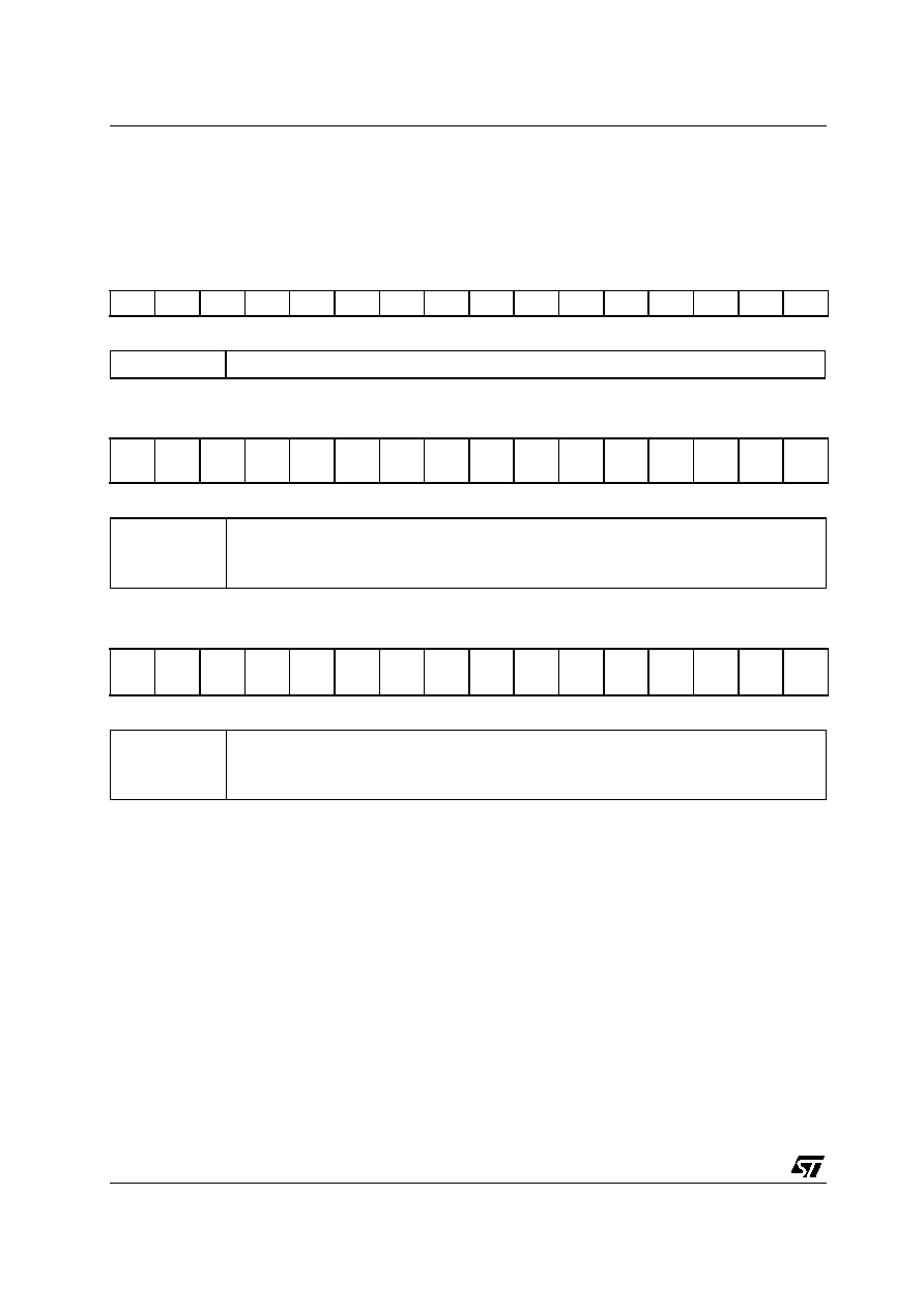
P2 (FFC0h / E0h)
SFR
Reset Value: 0000h
DP2 (FFC2h / E1h)
SFR
Reset Value: 0000h
ODP2 (F1C2h / E1h)
ESFR
Reset Value: 0000h
12.5.1 - Alternate Functions of Port 2
All Port 2 lines (P2.15...P2.0) serve as capture
inputs or compare outputs (CC15IO...CC0IO) for
the CAPCOM1 unit.
When a Port 2 line is used as a capture input, the
state of the input latch, which represents the state
of the port pin, is directed to the CAPCOM unit via
the line “Alternate Pin Data Input”. If an external
capture trigger signal is used, the direction of the
respective pin must be set to input.
If the direction is set to output, the state of the port
output latch will be read since the pin represents
the state of the output latch.
This can be used to trigger a capture event
through software by setting or clearing the port
latch. Note that in the output configuration, no
external device may drive the pin, otherwise
conflicts would occur.
When a Port 2 line is used as a compare output
(compare modes 1 and 3), the compare event (or
the timer overflow in compare mode 3) directly
effects the port output latch. In compare mode 1,
when a valid compare match occurs, the state of
the port output latch is read by the CAPCOM
control hardware via the line “Alternate Latch Data
Input”, inverted, and written back to the latch via
the line “Alternate Data Output”.
The port output latch is clocked by the signal
“Compare Trigger” which is generated by the
CAPCOM unit. In compare mode 3, when a match
occurs, the value '1' is written to the port output
latch via the line “Alternate Data Output”. When
an overflow of the corresponding timer occurs, a
'0' is written to the port output latch. In both cases,
15
14
13
12
11
10
98
765
432
10
P2.15 P2.14 P2.13 P2.12 P2.11 P2.10
P2.9
P2.8
P2.7
P2.6
P2.5
P2.4
P2.3
P2.2
P2.1
P2.0
RW
P2.y
Port Data Register P2 Bit y
15
14
13
12
11
10
98
765
432
10
DP2
.15
DP2
.14
DP2
.13
DP2
.12
DP2
.11
DP2
.10
DP2
.9
DP2
.8
DP2
.7
DP2
.6
DP2
.5
DP2
.4
DP2
.3
DP2
.2
DP2
.1
DP2
.0
RW
DP2.y
Port Direction Register DP2 Bit y
DP2.y = 0: Port line P2.y is an input (high-impedance)
DP2.y = 1: Port line P2.y is an output
15
14
13
12
11
10
98
765
432
10
ODP2
.15
ODP2
.14
ODP2
.13
ODP2
.12
ODP2
.11
ODP2
.10
ODP2
.9
ODP2
.8
ODP2
.7
ODP2
.6
ODP2
.5
ODP2
.4
ODP2
.3
ODP2
.2
ODP2
.1
ODP2
.0
RW
ODP2.y
Port 2 Open Drain Control Register Bit y
ODP2.y = 0: Port line P2.y output driver in push/pull mode
ODP2.y = 1: Port line P2.y output driver in open drain mode
相关PDF资料 |
PDF描述 |
|---|---|
| ST10F276Z5Q3 | 16-BIT, MROM, 64 MHz, RISC MICROCONTROLLER, PQFP144 |
| ST10F296TR | 16-BIT, FLASH, 64 MHz, MICROCONTROLLER, PBGA208 |
| ST10R172LT6 | 16-BIT, 50 MHz, MICROCONTROLLER, PQFP100 |
| ST10R272LT6 | 16-BIT, 50 MHz, MICROCONTROLLER, PQFP100 |
| ST16C452PSIJ68 | 2 CHANNEL(S), SERIAL COMM CONTROLLER, PQCC68 |
相关代理商/技术参数 |
参数描述 |
|---|---|
| ST10F269Z2Q6/TR | 功能描述:16位微控制器 - MCU 16B MCU 256K Byte and 12K Byte RAM RoHS:否 制造商:Texas Instruments 核心:RISC 处理器系列:MSP430FR572x 数据总线宽度:16 bit 最大时钟频率:24 MHz 程序存储器大小:8 KB 数据 RAM 大小:1 KB 片上 ADC:Yes 工作电源电压:2 V to 3.6 V 工作温度范围:- 40 C to + 85 C 封装 / 箱体:VQFN-40 安装风格:SMD/SMT |
| ST10F269Z2QX | 制造商:STMICROELECTRONICS 制造商全称:STMicroelectronics 功能描述:16-BIT MCU WITH MAC UNIT, 256K BYTE FLASH MEMORY AND 12K BYTE RAM |
| ST10F269Z2T3 | 功能描述:16位微控制器 - MCU ST10F272 16B MCU RoHS:否 制造商:Texas Instruments 核心:RISC 处理器系列:MSP430FR572x 数据总线宽度:16 bit 最大时钟频率:24 MHz 程序存储器大小:8 KB 数据 RAM 大小:1 KB 片上 ADC:Yes 工作电源电压:2 V to 3.6 V 工作温度范围:- 40 C to + 85 C 封装 / 箱体:VQFN-40 安装风格:SMD/SMT |
| ST10F269Z2T6 | 功能描述:16位微控制器 - MCU ST10F272 16B MCU RoHS:否 制造商:Texas Instruments 核心:RISC 处理器系列:MSP430FR572x 数据总线宽度:16 bit 最大时钟频率:24 MHz 程序存储器大小:8 KB 数据 RAM 大小:1 KB 片上 ADC:Yes 工作电源电压:2 V to 3.6 V 工作温度范围:- 40 C to + 85 C 封装 / 箱体:VQFN-40 安装风格:SMD/SMT |
| ST10F269ZX | 制造商:STMICROELECTRONICS 制造商全称:STMicroelectronics 功能描述:16-BIT MCU WITH MAC UNIT, 128K to 256K BYTE FLASH MEMORY AND 12K BYTE RAM |
发布紧急采购,3分钟左右您将得到回复。