- 您现在的位置:买卖IC网 > PDF目录98143 > ST10F269Z2Q6 (STMICROELECTRONICS) 16-BIT, FLASH, 40 MHz, MICROCONTROLLER, PQFP144 PDF资料下载
参数资料
| 型号: | ST10F269Z2Q6 |
| 厂商: | STMICROELECTRONICS |
| 元件分类: | 微控制器/微处理器 |
| 英文描述: | 16-BIT, FLASH, 40 MHz, MICROCONTROLLER, PQFP144 |
| 封装: | 28 X 28 MM, PLASTIC, QFP-144 |
| 文件页数: | 51/184页 |
| 文件大小: | 3276K |
| 代理商: | ST10F269Z2Q6 |
第1页第2页第3页第4页第5页第6页第7页第8页第9页第10页第11页第12页第13页第14页第15页第16页第17页第18页第19页第20页第21页第22页第23页第24页第25页第26页第27页第28页第29页第30页第31页第32页第33页第34页第35页第36页第37页第38页第39页第40页第41页第42页第43页第44页第45页第46页第47页第48页第49页第50页当前第51页第52页第53页第54页第55页第56页第57页第58页第59页第60页第61页第62页第63页第64页第65页第66页第67页第68页第69页第70页第71页第72页第73页第74页第75页第76页第77页第78页第79页第80页第81页第82页第83页第84页第85页第86页第87页第88页第89页第90页第91页第92页第93页第94页第95页第96页第97页第98页第99页第100页第101页第102页第103页第104页第105页第106页第107页第108页第109页第110页第111页第112页第113页第114页第115页第116页第117页第118页第119页第120页第121页第122页第123页第124页第125页第126页第127页第128页第129页第130页第131页第132页第133页第134页第135页第136页第137页第138页第139页第140页第141页第142页第143页第144页第145页第146页第147页第148页第149页第150页第151页第152页第153页第154页第155页第156页第157页第158页第159页第160页第161页第162页第163页第164页第165页第166页第167页第168页第169页第170页第171页第172页第173页第174页第175页第176页第177页第178页第179页第180页第181页第182页第183页第184页
ST10F269
144/184
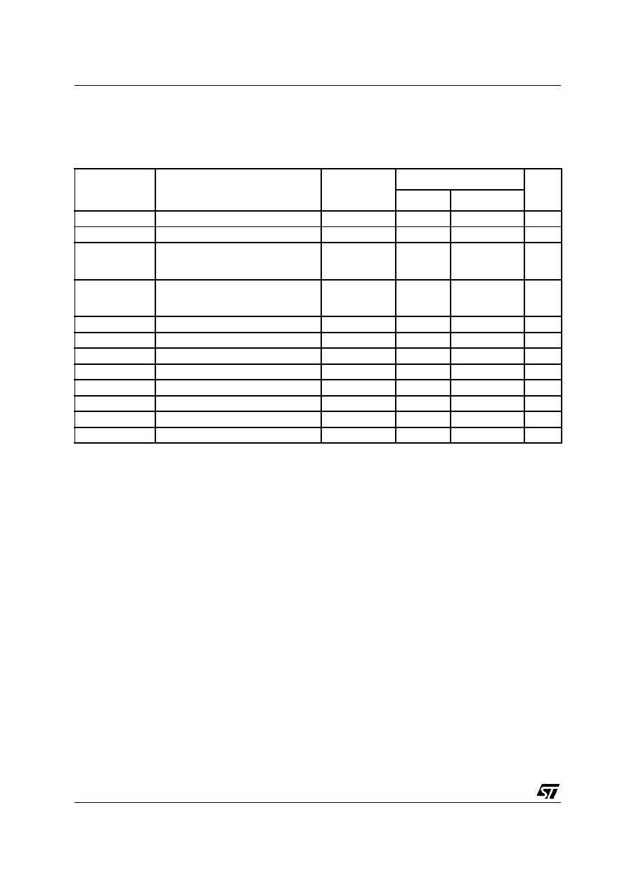
21.3.1 - A/D Converter Characteristics
VDD = 5V ± 10%, VSS = 0V, TA = -40 to +85°C or -40 to +125°C, 4.0V ≤ VAREF ≤ VDD + 0.1V; VSS0.1V ≤
VAGND ≤ VSS + 0.2V
Notes: 1. VAIN may exceed VAGND or VAREF up to the absolute maximum ratings. However, the conversion result in these cases will be
X000h or X3FFh, respectively.
2. During the tS sample time the input capacitance Cain can be charged/discharged by the external source. The internal resistance of
the analog source must allow the capacitance to reach its final voltage level within the tS sample time. After the end of the tS sample
time, changes of the analog input voltage have no effect on the conversion result. Values for the tSC sample clock depend on the
programming. Referring to the tC conversion time formula of Section 21.3.2 - ‘Conversion Timing Control’ on page 145 and to
- tS min. = 2 tSC min. = 2 tCC min. = 2 x 24 x TCL = 48 TCL
- tS max = 2 tSC max = 2 x 8 tCC max = 2 x 8 x 96 TCL = 1536 TCL
TCL is defined in Section 21.4.2 -, Section 21.4.4 -, and Section 21.4.5 - ‘Direct Drive’ on page 149:
3. The conversion time formula is:
- tC = 14 tCC + tS + 4 TCL (= 14 tCC + 2 tSC + 4 TCL)
The tC parameter includes the tS sample time, the time for determining the digital result and the time to load the result register with
the result of the conversion. Values for the tCC conversion clock depend on the programming. Referring to Table 42 on page 145:
- tC min. = 14 tCC min. + tS min. + 4 TCL = 14 x 24 x TCL + 48 TCL + 4 TCL = 388 TCL
- tC max = 14 tCC max + tS max + 4 TCL = 14 x 96 TCL + 1536 TCL + 4 TCL = 2884 TCL
4. This parameter is fixed by ADC control logic.
5. DNL, INL, TUE are tested at VAREF =5.0V, VAGND =0V, VCC = 4.9V. It is guaranteed by design characterization for all other
voltages within the defined voltage range.
‘LSB’ has a value of VAREF / 1024.
The specified TUE is guaranteed only if an overload condition (see
IOV specification) occurs on maximum 2 not selected analog input
pins and the absolute sum of input overload currents on all analog input pins does not exceed 10mA.
6. The coupling factor is measured on a channel while an overload condition occurs on the adjacent not selected channel with an
absolute overload current less than 10mA.
7. Partially tested, guaranteed by design characterization.
8.To remove noise and undesirable high frequency components from the analog input signal, a low-pass filter must be connected at
the ADC input. The cut-off frequency of this filter should avoid 2 opposite transitions during the ts sampling time of the ST10 ADC:
- fcut-off ≤ 1 / 5 ts to 1/10 ts
where ts is the sampling time of the ST10 ADC and is not related to the Nyquist frequency determined by the tc conversion time.
Table 41 : A/D Converter Characteristics
Symbol
Parameter
Test Condition
Limit Values
Unit
minimum
maximum
VAREF
SR
Analog Reference voltage
4.0
VDD + 0.1
V
VAIN
SR
Analog input voltage
1 - 8
VAGND
VAREF
V
IAREF
CC
Reference supply current
running mode
power-down mode
7
–
500
1
A
CAIN
CC
ADC input capacitance
Not sampling
Sampling
7
–
10
15
pF
tS
CC
Sample time
2 - 4
48 TCL
1 536 TCL
tC
CC
Conversion time
3 - 4
388 TCL
2 884 TCL
DNL
CC
Differential Nonlinearity
5
-0.5
+0.5
LSB
INL
CC
Integral Nonlinearity
5
-1.5
+1.5
LSB
OFS
CC
Offset Error
5
-1.0
+1.0
LSB
TUE
CC
Total unadjusted error
5
-2.0
+2.0
LSB
RASRC
SR
Internal resistance of analog source
tS in [ns]
2 - 7
–(tS / 150) - 0.25
k
K
CC
Coupling Factor between inputs
6 - 7
–1/500
相关PDF资料 |
PDF描述 |
|---|---|
| ST10F276Z5Q3 | 16-BIT, MROM, 64 MHz, RISC MICROCONTROLLER, PQFP144 |
| ST10F296TR | 16-BIT, FLASH, 64 MHz, MICROCONTROLLER, PBGA208 |
| ST10R172LT6 | 16-BIT, 50 MHz, MICROCONTROLLER, PQFP100 |
| ST10R272LT6 | 16-BIT, 50 MHz, MICROCONTROLLER, PQFP100 |
| ST16C452PSIJ68 | 2 CHANNEL(S), SERIAL COMM CONTROLLER, PQCC68 |
相关代理商/技术参数 |
参数描述 |
|---|---|
| ST10F269Z2Q6/TR | 功能描述:16位微控制器 - MCU 16B MCU 256K Byte and 12K Byte RAM RoHS:否 制造商:Texas Instruments 核心:RISC 处理器系列:MSP430FR572x 数据总线宽度:16 bit 最大时钟频率:24 MHz 程序存储器大小:8 KB 数据 RAM 大小:1 KB 片上 ADC:Yes 工作电源电压:2 V to 3.6 V 工作温度范围:- 40 C to + 85 C 封装 / 箱体:VQFN-40 安装风格:SMD/SMT |
| ST10F269Z2QX | 制造商:STMICROELECTRONICS 制造商全称:STMicroelectronics 功能描述:16-BIT MCU WITH MAC UNIT, 256K BYTE FLASH MEMORY AND 12K BYTE RAM |
| ST10F269Z2T3 | 功能描述:16位微控制器 - MCU ST10F272 16B MCU RoHS:否 制造商:Texas Instruments 核心:RISC 处理器系列:MSP430FR572x 数据总线宽度:16 bit 最大时钟频率:24 MHz 程序存储器大小:8 KB 数据 RAM 大小:1 KB 片上 ADC:Yes 工作电源电压:2 V to 3.6 V 工作温度范围:- 40 C to + 85 C 封装 / 箱体:VQFN-40 安装风格:SMD/SMT |
| ST10F269Z2T6 | 功能描述:16位微控制器 - MCU ST10F272 16B MCU RoHS:否 制造商:Texas Instruments 核心:RISC 处理器系列:MSP430FR572x 数据总线宽度:16 bit 最大时钟频率:24 MHz 程序存储器大小:8 KB 数据 RAM 大小:1 KB 片上 ADC:Yes 工作电源电压:2 V to 3.6 V 工作温度范围:- 40 C to + 85 C 封装 / 箱体:VQFN-40 安装风格:SMD/SMT |
| ST10F269ZX | 制造商:STMICROELECTRONICS 制造商全称:STMicroelectronics 功能描述:16-BIT MCU WITH MAC UNIT, 128K to 256K BYTE FLASH MEMORY AND 12K BYTE RAM |
发布紧急采购,3分钟左右您将得到回复。