- 您现在的位置:买卖IC网 > PDF目录98158 > TAS3218IPZPR (TEXAS INSTRUMENTS INC) SPECIALTY CONSUMER CIRCUIT, PQFP100 PDF资料下载
参数资料
| 型号: | TAS3218IPZPR |
| 厂商: | TEXAS INSTRUMENTS INC |
| 元件分类: | 消费家电 |
| 英文描述: | SPECIALTY CONSUMER CIRCUIT, PQFP100 |
| 封装: | GREEN, PLASTIC, TQFP-100 |
| 文件页数: | 42/79页 |
| 文件大小: | 1263K |
| 代理商: | TAS3218IPZPR |
第1页第2页第3页第4页第5页第6页第7页第8页第9页第10页第11页第12页第13页第14页第15页第16页第17页第18页第19页第20页第21页第22页第23页第24页第25页第26页第27页第28页第29页第30页第31页第32页第33页第34页第35页第36页第37页第38页第39页第40页第41页当前第42页第43页第44页第45页第46页第47页第48页第49页第50页第51页第52页第53页第54页第55页第56页第57页第58页第59页第60页第61页第62页第63页第64页第65页第66页第67页第68页第69页第70页第71页第72页第73页第74页第75页第76页第77页第78页第79页
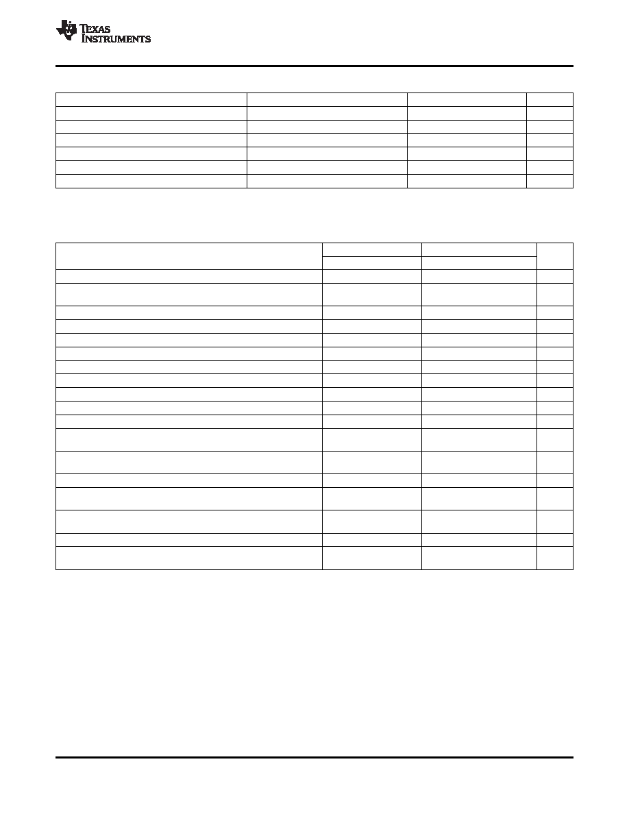
SPDIF INTERFACE SIGNALS TIMING CHARACTERISTICS
I
2C INTERFACE AND I/O CHARACTERISTICS OF THE SDA AND SCL BUS LINES FOR
www.ti.com ....................................................................................................................................................................................................... SLES235 – JULY 2008
PARAMETER
TEST CONDITIONS
MIN
TYP
MAX
UNIT
Fs
Encoded data sampling rate
32
48
kHz
Rspdif
SPDIF signal bitrate
128 Fs
MHz
UI
Unit interval
1/Rspdif
ns
TLO/THI
Low/high periods
1 UI
3 UI
ns
VOH
High-level output voltage
3.3-V TTL, IOH = 4 mA
2.4
V
VOL
Low-level output voltage
3.3-V TTL, IOL = 4 mA
0.5
V
STANDARD- AND FAST-MODE I
2C BUS DEVICES
See Figure 38
PARAMETER
STANDARD MODE
FAST MODE
UNIT
MIN
MAX
MIN
MAX
fSCL
SCL clock frequency
0
100
0
400(1)
kHz
Hold time (repeated) START condition. After this period,
tHD;STA
4
0.6
s
the first clock pulse is generated.
tLOW
LOW period of the SCL clock
4.7
1.3
s
tHIGH
HIGH period of the SCL clock
4
0.6
s
tsu;STA
Set-up time for a repeated START condition
4.7
0.6
s
tsu;DAT
Data set-up time
250
100(2)
ns
tr
Rise time of both SDA and SCL signals
1000
20 + 0.1 Cb
(3)
300
ns
tf
Fall time of both SDA and SCL signals
300
20 + 0.1 Cb
(3)
300
ns
tsu;STO
Set-up time for STOP condition
4
0.6
s
tBUF
Bus free time between a STOP and START condition
4.7
1.3
s
Cb
Capacitive load for each bus line
400
pF
Noise margin at the LOW level for each connected device
VnL
0.1 VDD
V
(including hysteresis)
Noise margin at the HIGH level for each connected device
VnH
0.2 VDD
V
(including hysteresis)
Vhys
Hysteresis of Schmitt trigger inputs
0.05 VDD
V
Pulse width of spikes which must be suppressed by the
tSP
0
50
ns
input filter
Input current each I/O pin with an input voltage between
Ii
10
10(4)
A
0.1 VDD and 0.9 VDD max
Ci
Capacitance for each I/O pin
10
pF
Output fall time from VIHmin to VILmax with a bus
tof
250(5)
7 + 0.1 Cb
(3)
250(5)
ns
capacitance from 10 pF to 400 pF
(1)
In Master mode the maximum I2C clock rate is 375 kHz.
(2)
A Fast-mode I2C bus device can be used in a Standard-mode I2C bus system, but the requirement tSU;DAT 250 ns must then be met.
This will automatically be the case if the device does not stretch the LOW period of the SCL signal. If such a device does stretch the
LOW period of the SCL signal, it must output the next data bit to the SDA line.
(3)
Cb = total capacitance of one bus line in pF.
(4)
I/O pins of Fast-mode devices must not obstruct the SDA and SCL lines if VDD is switched off.
(5)
The maximum tf for the SDA and SCL bus lines (300 ns) is longer than the specified maximum tof for the output stages (250 ns). This
allows series protection resistors (Rs) to be connected between the SDA/SCL pins and the SDA/SCL bus lines without exceeding the
maximum specified tf.
Copyright 2008, Texas Instruments Incorporated
47
Product Folder Link(s): TAS3218
相关PDF资料 |
PDF描述 |
|---|---|
| TAS3218IPZP | SPECIALTY CONSUMER CIRCUIT, PQFP100 |
| TAS3218PZPR | SPECIALTY CONSUMER CIRCUIT, PQFP100 |
| TAS3218PZP | SPECIALTY CONSUMER CIRCUIT, PQFP100 |
| TAS5000PFB | SPECIALTY CONSUMER CIRCUIT, PQFP48 |
| TAS5000PFBG4 | SPECIALTY CONSUMER CIRCUIT, PQFP48 |
相关代理商/技术参数 |
参数描述 |
|---|---|
| TAS3218PZP | 功能描述:音频 DSP Dig Audio SoC for multi-channel app RoHS:否 制造商:Texas Instruments 工作电源电压: 电源电流: 工作温度范围: 安装风格: 封装 / 箱体: 封装:Tube |
| TAS3218PZPR | 功能描述:音频 DSP Dig Audio SoC for multi-channel app RoHS:否 制造商:Texas Instruments 工作电源电压: 电源电流: 工作温度范围: 安装风格: 封装 / 箱体: 封装:Tube |
| TAS-3225A | 制造商:TEW 功能描述: |
| TAS-3225A 44.000KHZ | 制造商:TEW 功能描述: |
| TAS-3225J 13.56MHz }20ppm/22pF | 制造商:Tokyo Denpa 功能描述:13.560000MHz }20ppm }15ppm 22pF 3.2~2.5~0.55mm +85 -30 3.2mm 2.5mm 0.55mm Cut Tape |
发布紧急采购,3分钟左右您将得到回复。