- 您现在的位置:买卖IC网 > PDF目录19457 > TMS320VC5409PGE-80 (Texas Instruments)IC FIXED POINT DSP 144-LQFP PDF资料下载
参数资料
| 型号: | TMS320VC5409PGE-80 |
| 厂商: | Texas Instruments |
| 文件页数: | 30/93页 |
| 文件大小: | 0K |
| 描述: | IC FIXED POINT DSP 144-LQFP |
| 标准包装: | 60 |
| 系列: | TMS320C54x |
| 类型: | 定点 |
| 接口: | 主机接口,McBSP |
| 时钟速率: | 80MHz |
| 非易失内存: | ROM(32 kB) |
| 芯片上RAM: | 64kB |
| 电压 - 输入/输出: | 3.30V |
| 电压 - 核心: | 1.80V |
| 工作温度: | -40°C ~ 100°C |
| 安装类型: | 表面贴装 |
| 封装/外壳: | 144-LQFP |
| 供应商设备封装: | 144-LQFP(20x20) |
| 包装: | 托盘 |
| 配用: | 296-15829-ND - DSP STARTER KIT FOR TMS320C5416 |
第1页第2页第3页第4页第5页第6页第7页第8页第9页第10页第11页第12页第13页第14页第15页第16页第17页第18页第19页第20页第21页第22页第23页第24页第25页第26页第27页第28页第29页当前第30页第31页第32页第33页第34页第35页第36页第37页第38页第39页第40页第41页第42页第43页第44页第45页第46页第47页第48页第49页第50页第51页第52页第53页第54页第55页第56页第57页第58页第59页第60页第61页第62页第63页第64页第65页第66页第67页第68页第69页第70页第71页第72页第73页第74页第75页第76页第77页第78页第79页第80页第81页第82页第83页第84页第85页第86页第87页第88页第89页第90页第91页第92页第93页
Functional Overview
36
April 1999 Revised October 2008
SPRS082F
3.3.2.2
McBSP Control Registers and Subaddresses
The control registers for the multichannel buffered serial port (McBSP) are accessed using the subbank
addressing scheme. This allows a set or subbank of registers to be accessed through a single memory
location. The serial port subbank address (SPSA) register is used as a pointer to select a particular register
within the subbank. The serial port subbank data (SPSD) register is used to access (read or write) the selected
register. Table 310 shows the McBSP control registers and their corresponding subaddresses.
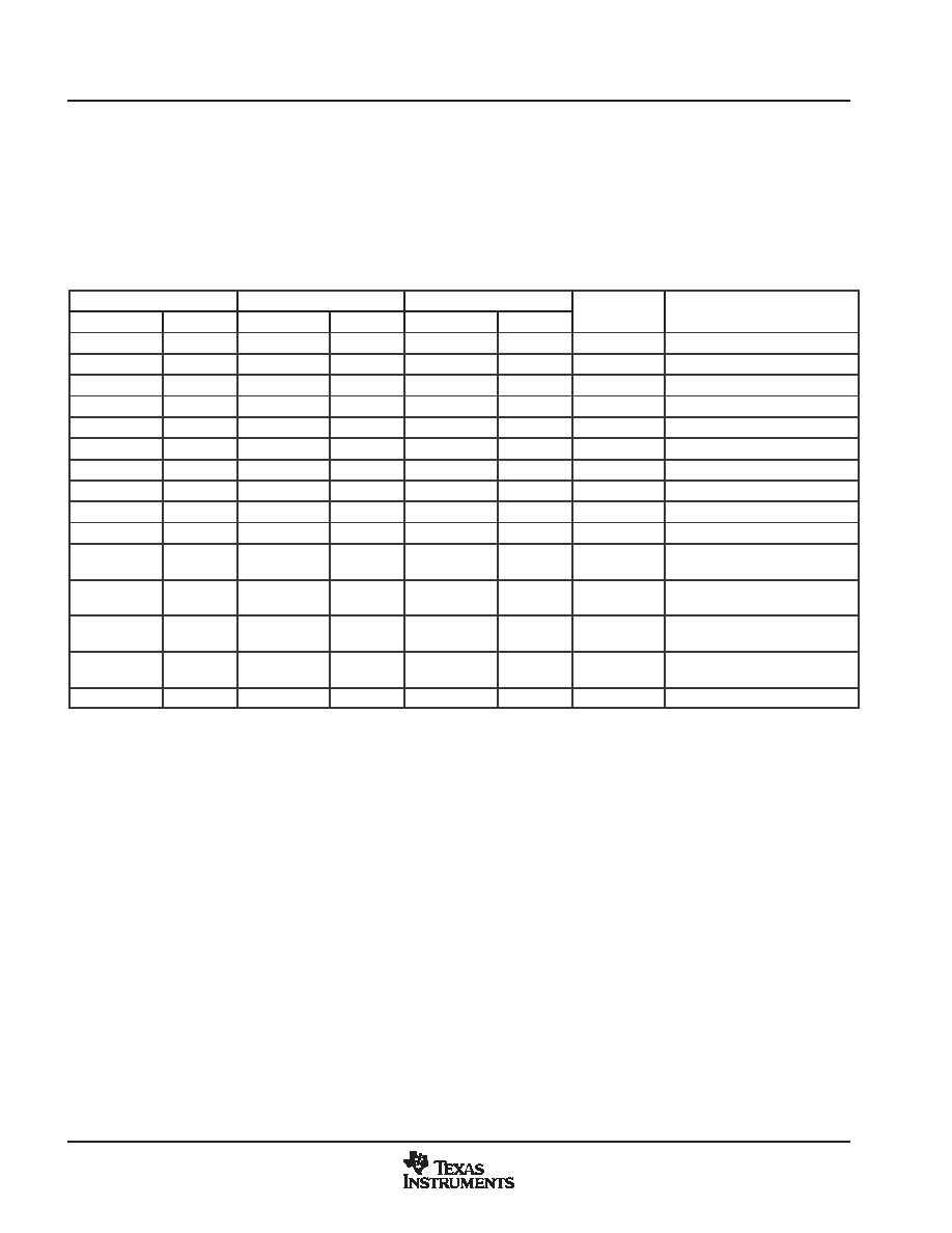
Table 310. McBSP Control Registers and Subaddresses
McBSP0
McBSP1
McBSP2
SUB
DESCRIPTION
NAME
ADDRESS
NAME
ADDRESS
NAME
ADDRESS
SUB
ADDRESS
DESCRIPTION
SPCR10
39h
SPCR11
49h
SPCR12
35h
00h
Serial port control register 1
SPCR20
39h
SPCR21
49h
SPCR22
35h
01h
Serial port control register 2
RCR10
39h
RCR11
49h
RCR12
35h
02h
Receive control register 1
RCR20
39h
RCR21
49h
RCR22
35h
03h
Receive control register 2
XCR10
39h
XCR11
49h
XCR12
35h
04h
Transmit control register 1
XCR20
39h
XCR21
49h
XCR22
35h
05h
Transmit control register 2
SRGR10
39h
SRGR11
49h
SRGR12
35h
06h
Sample rate generator register 1
SRGR20
39h
SRGR21
49h
SRGR22
35h
07h
Sample rate generator register 2
MCR10
39h
MCR11
49h
MCR12
35h
08h
Multichannel register 1
MCR20
39h
MCR21
49h
MCR22
35h
09h
Multichannel register 2
RCERA0
39h
RCERA1
49h
RCERA2
35h
0Ah
Receive channel enable register
partition A
RCERB0
39h
RCERB1
49h
RCERB2
35h
0Bh
Receive channel enable register
partition B
XCERA0
39h
XCERA1
49h
XCERA2
35h
0Ch
Transmit channel enable register
partition A
XCERB0
39h
XCERB1
49h
XCERB2
35h
0Dh
Transmit channel enable register
partition B
PCR0
39h
PCR1
49h
PCR2
35h
0Eh
Pin control register
3.3.3 Hardware Timer
The 5409 device features one 16-bit timing circuit with a 4-bit prescaler. The main counter of each timer is
decremented by one every CPU clock cycle. Each time the counter decrements to 0, a timer interrupt is
generated. The timer can be stopped, restarted, reset, or disabled by specific control bits.
3.3.4 Clock Generator
The clock generator provides clocks to the 5409 device, and consists of an internal oscillator and a
phase-locked loop (PLL) circuit. The clock generator requires a reference clock input, which can be provided
by using a crystal resonator with the internal oscillator, or from an external clock source. The reference clock
input is then divided by two (DIV mode) to generate clocks for the 5409 device, or the PLL circuit can be used
(PLL mode) to generate the device clock by multiplying the reference clock frequency by a scale factor,
allowing use of a clock source with a lower frequency than that of the CPU.The PLL is an adaptive circuit that,
once synchronized, locks onto and tracks an input clock signal.
When the PLL is initially started, it enters a transitional mode during which the PLL acquires lock with the input
signal. Once the PLL is locked, it continues to track and maintain synchronization with the input signal. Then,
other internal clock circuitry allows the synthesis of new clock frequencies for use as master clock for the 5409
device.
相关PDF资料 |
PDF描述 |
|---|---|
| RSA06DTKH | CONN EDGECARD 12POS DIP .125 SLD |
| VJ1206Y681KBEAT4X | CAP CER 680PF 500V 10% X7R 1206 |
| 172-015-102R011 | CONN DB15 MALE SOLDER CUP TIN |
| BWR-15/670-D12A-C | CONV DC/DC +/-15V +/-670MA DIP |
| VJ1206Y682KBAAT4X | CAP CER 6800PF 50V 10% X7R 1206 |
相关代理商/技术参数 |
参数描述 |
|---|---|
| TMS320VC5409ZGU100 | 功能描述:数字信号处理器和控制器 - DSP, DSC Fixed-Pt Dig Signal Proc RoHS:否 制造商:Microchip Technology 核心:dsPIC 数据总线宽度:16 bit 程序存储器大小:16 KB 数据 RAM 大小:2 KB 最大时钟频率:40 MHz 可编程输入/输出端数量:35 定时器数量:3 设备每秒兆指令数:50 MIPs 工作电源电压:3.3 V 最大工作温度:+ 85 C 封装 / 箱体:TQFP-44 安装风格:SMD/SMT |
| TMS320VC5409ZGU-80 | 功能描述:数字信号处理器和控制器 - DSP, DSC Fixed-Pt Dig Signal Proc RoHS:否 制造商:Microchip Technology 核心:dsPIC 数据总线宽度:16 bit 程序存储器大小:16 KB 数据 RAM 大小:2 KB 最大时钟频率:40 MHz 可编程输入/输出端数量:35 定时器数量:3 设备每秒兆指令数:50 MIPs 工作电源电压:3.3 V 最大工作温度:+ 85 C 封装 / 箱体:TQFP-44 安装风格:SMD/SMT |
| TMS320VC5410AGGU1 | 制造商:Rochester Electronics LLC 功能描述:- Bulk 制造商:Texas Instruments 功能描述: |
| TMS320VC5410AGGU12 | 功能描述:数字信号处理器和控制器 - DSP, DSC Dig Signal Proc RoHS:否 制造商:Microchip Technology 核心:dsPIC 数据总线宽度:16 bit 程序存储器大小:16 KB 数据 RAM 大小:2 KB 最大时钟频率:40 MHz 可编程输入/输出端数量:35 定时器数量:3 设备每秒兆指令数:50 MIPs 工作电源电压:3.3 V 最大工作温度:+ 85 C 封装 / 箱体:TQFP-44 安装风格:SMD/SMT |
| TMS320VC5410AGGU16 | 功能描述:数字信号处理器和控制器 - DSP, DSC Dig Signal Proc RoHS:否 制造商:Microchip Technology 核心:dsPIC 数据总线宽度:16 bit 程序存储器大小:16 KB 数据 RAM 大小:2 KB 最大时钟频率:40 MHz 可编程输入/输出端数量:35 定时器数量:3 设备每秒兆指令数:50 MIPs 工作电源电压:3.3 V 最大工作温度:+ 85 C 封装 / 箱体:TQFP-44 安装风格:SMD/SMT |
发布紧急采购,3分钟左右您将得到回复。