- 您现在的位置:买卖IC网 > PDF目录17451 > TPS51020EVM-001 (Texas Instruments)EVAL MODULE FOR TPS51020-001 PDF资料下载
参数资料
| 型号: | TPS51020EVM-001 |
| 厂商: | Texas Instruments |
| 文件页数: | 7/28页 |
| 文件大小: | 0K |
| 描述: | EVAL MODULE FOR TPS51020-001 |
| 标准包装: | 1 |
| 主要目的: | DC/DC,步降 |
| 输出及类型: | 2,非隔离 |
| 输出电压: | 3.3V,5V |
| 电流 - 输出: | 6A,6A |
| 输入电压: | 8 ~ 20 V |
| 稳压器拓扑结构: | 降压 |
| 频率 - 开关: | 300kHz |
| 板类型: | 完全填充 |
| 已供物品: | 板 |
| 已用 IC / 零件: | TPS51020 |
| 产品目录页面: | 1028 (CN2011-ZH PDF) |
| 相关产品: | TPS51020DBTRG4-ND - IC DUAL DC/DC SYNC CTRLR 30TSSOP 296-26971-2-ND - IC DUAL DC/DC SYNC CTRLR 30TSSOP TPS51020DBTG4-ND - IC DUAL DC/DC SYNC CTRLR 30TSSOP 296-15896-5-ND - IC DUAL DC/DC CTRLR SYNC 30TSSOP |
| 其它名称: | 296-18958 |
第1页第2页第3页第4页第5页第6页当前第7页第8页第9页第10页第11页第12页第13页第14页第15页第16页第17页第18页第19页第20页第21页第22页第23页第24页第25页第26页第27页第28页
�� �
�
�TPS51020�
�SLUS564C� ?� JULY� 2003� ?� REVISED� OCTOBER� 2008�
�ENBL1�
�ENBL1�
�470�
�ENBL2�
�5.0�
�3.6�
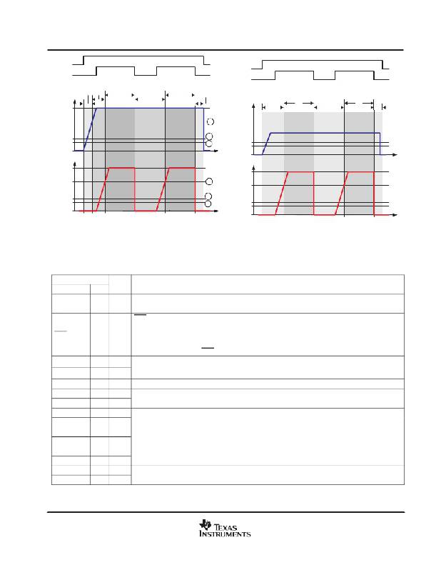
�fSW� ?� Switching� Frequency� ?� kHz�
�27� 0 36 0�
�4� 70�
�36� 0�
�SSTRT1�
�27� 0�
�C�
�ENBL2�
�5.0�
�3.6�
�fSW� ?� Switching� Frequency� ?� kHz�
�36� 0 36 0�
�27� 0 27 0�
�SSTRT1�
�27� 0�
�1.5�
�1.2�
�0�
�B�
�A�
�1.5�
�1.2�
�0�
�5.0�
�3.6�
�SSTRT2�
�C�
�5.0�
�3.6�
�SSTRT2�
�B�
�1.5�
�1.2�
�0�
�t0� t1�
�t2�
�t3�
�t4�
�t5�
�A�
�1.5�
�1.2�
�0�
�t0� t1�
�t2�
�t3�
�t4�
�t5�
�t� ?� Time�
�RSSTRT1� =� RSSTRT2� =� OPEN� =� 450� kHz�
�Figure� 1�
�TERMINAL� FUNCTIONS�
�TERMINAL�
�t� ?� Time�
�RSSTRT1� =� 1� M� ?� ,� RSSTRT2� =� OPEN� =� 360� kHz�
�Figure� 2�
�NAME�
�COMP1�
�COMP2�
�NO.�
�2�
�14�
�I/O�
�O�
�O�
�DESCRIPTION�
�Error� amplifier� output.� Connect� feedback� network� to� this� pin� and� INVx� for� compensation� of� control� loop.�
�DDR� selection� pin.� If� this� pin� is� grounded,� the� device� runs� in� DDR� Mode.� The� error� amplifier� reference� for� VO2�
�is� (VO1_VDDQ)/2,� the� REF_X� output� voltage� becomes� (VO1_VDDQ)/2� and� skip� mode� is� disabled� for� VO2,�
�DDR�
�6�
�I�
�Also,� VREG5� is� turned� off� when� both� ENBLx� are� at� low� in� this� mode.� If� this� pin� is� at� 2.2-V� or� higher,� the� device�
�runs� in� ordinary� dual� SMPS� mode� (dual� mode),� then� the� error� amplifier� reference� for� VO2� is� connected� to� inter-�
�nal� 0.85-V� reference,� the� REF_X� output� voltage� becomes� 10� V,� V� REG5� is� kept� on� regardless� of� ENBLx� status.�
�CAUTION:� Do� not� toggle� DDR� while� ENBL1� or� ENBL2� are� high.� (See� Table� 2)�
�ENBL1�
�9�
�I�
�TTL� Enable� Input.� If� ENBLx� is� greater� than� 2.2� V,� then� the� VREG5� is� enabled� (DDR� mode)� and� the� SMPS� of�
�that� channel� attempts� to� turn� on.� If� both� ENBL1� and� ENBL2� are� low� then� the� 10-V� (or� (VO1_VDDQ)� /2� output)�
�ENBL2�
�GND�
�INV1�
�INV2�
�LL1�
�LL2�
�OUT1_D�
�OUT2_D�
�OUT1_U�
�OUT2_U�
�OUTGND1�
�OUTGND2�
�10�
�7�
�1�
�15�
�28�
�18�
�27�
�19�
�29�
�17�
�26�
�20�
�I�
�O�
�I�
�I�
�I/O�
�I/O�
�O�
�O�
�O�
�O�
�O�
�O�
�voltage� as� well� as� the� oscillator� are� turned� off.� (See� Table� 2)�
�Signal� ground� pin.�
�Error� amplifier� inverting� input.� Also� input� for� skip� comparator,� and� OVP/UVP� comparators.�
�Switch-node� connection� for� high-side� driver� and� overcurrent� protection� circuitry.�
�Synchronous� N-channel� MOSFET� driver� outp� ut.�
�High-side� N-channel� MOSFET� driver� outp� ut.�
�Ground return for OUTx_D.�
�www.ti.com�
�7�
�相关PDF资料 |
PDF描述 |
|---|---|
| 306XC104B | TRIMMER 100K OHM 0.5W TH |
| ECC07DRES-S13 | CONN EDGECARD 14POS .100 EXTEND |
| 306XC503B | TRIMMER 50K OHM 0.5W TH |
| HBC05DRYN | CONN EDGECARD 10POS DIP .100 SLD |
| 306XC203B | TRIMMER 20K OHM 0.5W TH |
相关代理商/技术参数 |
参数描述 |
|---|---|
| TPS5102DBT | 制造商:TI 制造商全称:Texas Instruments 功能描述:DUAL, HIGH-EFFICIENCY CONTROLLER FOR NOTEBOOK PC POWER |
| TPS5102IDBR | 制造商:未知厂家 制造商全称:未知厂家 功能描述:Analog IC |
| TPS5102IDBT | 功能描述:DC/DC 开关控制器 Dual Output Synch Buck Controller RoHS:否 制造商:Texas Instruments 输入电压:6 V to 100 V 开关频率: 输出电压:1.215 V to 80 V 输出电流:3.5 A 输出端数量:1 最大工作温度:+ 125 C 安装风格: 封装 / 箱体:CPAK |
| TPS5102IDBTG4 | 功能描述:DC/DC 开关控制器 Dual Output Synch Buck Cntrlr RoHS:否 制造商:Texas Instruments 输入电压:6 V to 100 V 开关频率: 输出电压:1.215 V to 80 V 输出电流:3.5 A 输出端数量:1 最大工作温度:+ 125 C 安装风格: 封装 / 箱体:CPAK |
| TPS5102IDBTR | 功能描述:DC/DC 开关控制器 Dual Output Synch Buck Cntrlr RoHS:否 制造商:Texas Instruments 输入电压:6 V to 100 V 开关频率: 输出电压:1.215 V to 80 V 输出电流:3.5 A 输出端数量:1 最大工作温度:+ 125 C 安装风格: 封装 / 箱体:CPAK |
发布紧急采购,3分钟左右您将得到回复。