- 您现在的位置:买卖IC网 > PDF目录275205 > V59C1G01164QAUF37H (PROMOS TECHNOLOGIES INC) 64M X 16 DDR DRAM, PBGA92 PDF资料下载
参数资料
| 型号: | V59C1G01164QAUF37H |
| 厂商: | PROMOS TECHNOLOGIES INC |
| 元件分类: | DRAM |
| 英文描述: | 64M X 16 DDR DRAM, PBGA92 |
| 封装: | ROHS COMPLIANT, FBGA-92 |
| 文件页数: | 55/79页 |
| 文件大小: | 1028K |
| 代理商: | V59C1G01164QAUF37H |
第1页第2页第3页第4页第5页第6页第7页第8页第9页第10页第11页第12页第13页第14页第15页第16页第17页第18页第19页第20页第21页第22页第23页第24页第25页第26页第27页第28页第29页第30页第31页第32页第33页第34页第35页第36页第37页第38页第39页第40页第41页第42页第43页第44页第45页第46页第47页第48页第49页第50页第51页第52页第53页第54页当前第55页第56页第57页第58页第59页第60页第61页第62页第63页第64页第65页第66页第67页第68页第69页第70页第71页第72页第73页第74页第75页第76页第77页第78页第79页
59
ProMOS TECHNOLOGIES
V59C1G01(408/808/168)QA
V59C1G01(408/808/168)QA Rev. 1.3 June 2008
NOTE 1 The typical value of VOX(AC) is expected to be about 0.5 x VDDQ of the transmitting
device and VOX(AC) is expected to track variations in VDDQ . VOX(AC) indicates the voltage at which
differential output signals must cross.
Overshoot/undershoot specification
Differential input AC logic level
Symbol
Parameter
Min.
Max.
Units
Notes
V
ID (ac)
ac differential input voltage
0.5
VDDQ + 0.6
V
1
V
IX (ac)
ac differential crosspoint voltage
0.5 x VDDQ - 0.175
0.5 x VDDQ + 0.175
V
2
Dif ferential AC output parameters
Symbol
Parameter
Min.
Max.
Units
Notes
V
OX (ac)
ac differential crosspoint voltage
0.5 x VDDQ - 0.125
0.5 x VDDQ + 0.125
V
1
AC overshoot/undershoot specification for address and control pins:
A0-A15, BA0-BA2, CS, RAS, CAS, WE, CKE, ODT
Parameter
Specification
DDR2-667
DDR2-800
Maximum peak amplitude allowed for overshoot area (See Figure 74):
0.5(0.9)1 V
Maximum peak amplitude allowed for undershoot area (See Figure 74):
0.5(0.9)1 V
Maximum overshoot area above VDD (See Figure 74).
0.8 V-ns
0.66 V-ns
Maximum undershoot area below VSS (See Figure 74).
0.8 V-ns
0.66 V-ns
NOTE 1
The maximum requirements for peak amplitude were reduced from 0.9V to 0.5V. Register vendor data sheets will spec-
ify the maximum over/undershoot induced in specific RDIMM applications. DRAM vendor data sheets will also specify the maxi-
mum overshoot/undershoot that their DRAM can tolerate. This will allow the RDIMM supplier to understand whether the DRAM
can tolerate the overshoot that the register will induce in the specific RDIMM application.
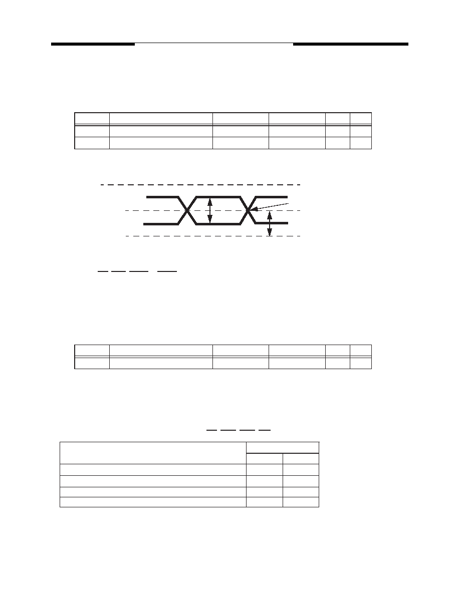
VDDQ
Crossing point
VSSQ
VTR
VCP
VID
VIX or VOX
Differenti al signal levels
NOTE 1
VID(AC) specifies the input differential voltage |VTR -VCP | required for switching, where VTR is
the true input signal (such as CK, DQS, LDQS or UDQS) and VCP is the complementary input signal
(such as CK, DQS, LDQS or UDQS). The minimum value is equal to V IH(AC) - V IL(AC).
NOTE 2
The typical value of VIX(AC) is expected to be about 0.5 x VDDQ of the transmitting device and
VIX(AC) is expected to track variations in VDDQ. VIX(AC) indicates the voltage at which differential input
signals must cross.
AC & DC operating conditions (cont'd)
相关PDF资料 |
PDF描述 |
|---|---|
| V59C1G01164QALJ19AE | 64M X 16 DDR DRAM, BGA92 |
| V59C1G01164QALF37I | 64M X 16 DDR DRAM, PBGA92 |
| V59C1G01164QALF25H | 64M X 16 DDR DRAM, PBGA92 |
| V62C2801024L-70VI | 128K X 8 STANDARD SRAM, 70 ns, PDSO32 |
| V58C2128804SBT5B | 16M X 8 DDR DRAM, 0.65 ns, PDSO66 |
相关代理商/技术参数 |
参数描述 |
|---|---|
| V5A010CB | 制造商:Honeywell Sensing and Control 功能描述:MICROSWITCH V5 PIN PLUNGER |
| V5A010CB | 制造商:Honeywell Sensing and Control 功能描述:MICROSWITCH V5 PIN PLUNGER |
| V5A010CB4D | 制造商:Honeywell Sensing and Control 功能描述:MICROSWITCH V5 ROLLER LEVER |
| V5A010CB4D | 制造商:Honeywell Sensing and Control 功能描述:MICROSWITCH V5 ROLLER LEVER |
| V5A010CB4E | 制造商:Honeywell Sensing and Control 功能描述:MICROSWITCH V5 ROLLER LEVER |
发布紧急采购,3分钟左右您将得到回复。