参数资料
| 型号: | W25Q40BWSNIG |
| 厂商: | Winbond Electronics |
| 文件页数: | 54/73页 |
| 文件大小: | 0K |
| 描述: | IC FLASH SPI 4MBIT 8SOIC |
| 标准包装: | 100 |
| 系列: | SpiFlash® |
| 格式 - 存储器: | 闪存 |
| 存储器类型: | FLASH |
| 存储容量: | 4M (512K x 8) |
| 速度: | 80MHz |
| 接口: | SPI 串行 |
| 电源电压: | 1.65 V ~ 1.95 V |
| 工作温度: | -40°C ~ 85°C |
| 封装/外壳: | 8-SOIC(0.154",3.90mm 宽) |
| 供应商设备封装: | 8-SOIC |
| 包装: | 管件 |
第1页第2页第3页第4页第5页第6页第7页第8页第9页第10页第11页第12页第13页第14页第15页第16页第17页第18页第19页第20页第21页第22页第23页第24页第25页第26页第27页第28页第29页第30页第31页第32页第33页第34页第35页第36页第37页第38页第39页第40页第41页第42页第43页第44页第45页第46页第47页第48页第49页第50页第51页第52页第53页当前第54页第55页第56页第57页第58页第59页第60页第61页第62页第63页第64页第65页第66页第67页第68页第69页第70页第71页第72页第73页
�� �
�
�W25Q40BW�
�8.2.36�
�Erase� Security� Registers� (44h)�
�The� W25Q40BW� offers� four� 256-byte� Security� Registers� which� can� be� erased� and� programmed�
�individually.� These� registers� may� be� used� by� the� system� manufacturers� to� store� security� and� other�
�important� information� separately� from� the� main� memory� array.�
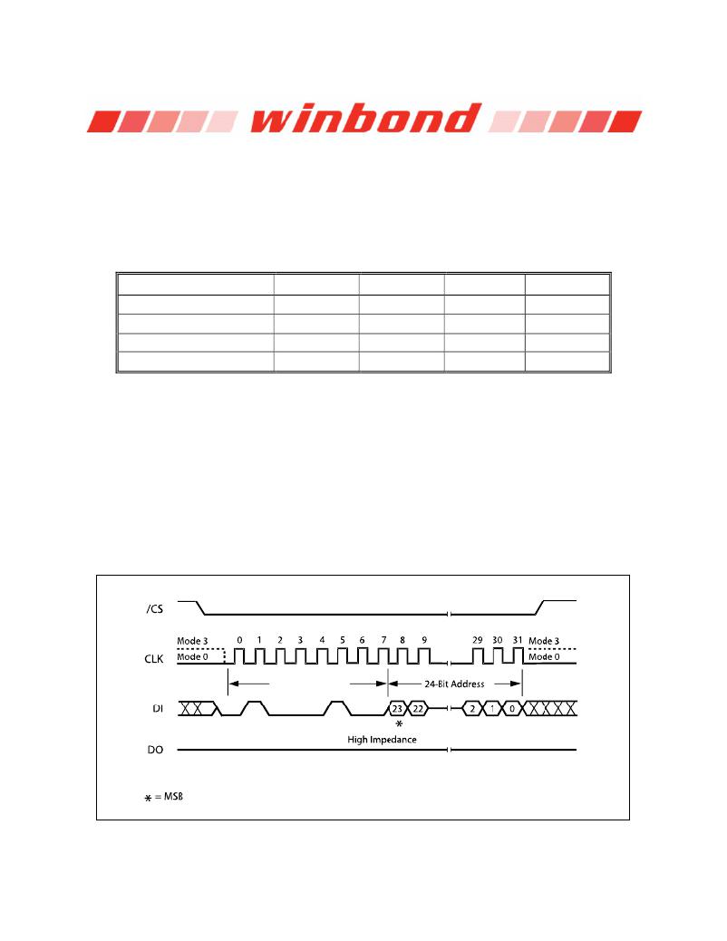
�The� Erase� Security� Register� instruction� is� similar� to� the� Sector� Erase� instruction.� A� Write� Enable�
�instruction� must� be� executed� before� the� device� will� accept� the� Erase� Security� Register� Instruction� (Status�
�Register� bit� WEL� must� equal� 1).� The� instruction� is� initiated� by� driving� the� /CS� pin� low� and� shifting� the�
�instruction� code� “� 44� h”� followed� by� a� 24-bit� address� (A23-A0)� to� erase� one� of� the� four� security� registers.�
�ADDRESS�
�Security� Register� #0*�
�Security� Register� #1�
�Security� Register� #2�
�Security� Register� #3�
�A23-16�
�00h�
�00h�
�00h�
�00h�
�A15-12�
�0000�
�0001�
�0010�
�0011�
�A11-8�
�0000�
�0000�
�0000�
�0000�
�A7-0�
�Don’t� Care�
�Don’t� Care�
�Don’t� Care�
�Don’t� Care�
�*� Please� note� that� Security� Register� 0� is� Reserved� by� Winbond� for� future� use.� It� is�
�recommended� to� use� Security� registers� 1-� 3� before� using� register� 0.�
�The� Erase� Security� Register� instruction� sequence� is� shown� in� figure� 34.� The� /CS� pin� must� be� driven� high�
�after� the� eighth� bit� of� the� last� byte� has� been� latched.� If� this� is� not� done� the� instruction� will� not� be� executed.�
�After� /CS� is� driven� high,� the� self-timed� Erase� Security� Register� operation� will� commence� for� a� time�
�duration� of� t� SE� (See� AC� Characteristics).� While� the� Erase� Security� Register� cycle� is� in� progress,� the� Read�
�Status� Register� instruction� may� still� be� accessed� for� checking� the� status� of� the� BUSY� bit.� The� BUSY� bit� is�
�a� 1� during� the� erase� cycle� and� becomes� a� 0� when� the� cycle� is� finished� and� the� device� is� ready� to� accept�
�other� instructions� again.� After� the� Erase� Security� Register� cycle� has� finished� the� Write� Enable� Latch�
�(WEL)� bit� in� the� Status� Register� is� cleared� to� 0.� The� Security� Register� Lock� Bits� (LB3-0)� in� the� Status�
�Register-2� can� be� used� to� OTP� protect� the� security� registers.� Once� a� lock� bit� is� set� to� 1,� the�
�corresponding� security� register� will� be� permanently� locked,� Erase� Security� Register� instruction� to� that�
�register� will� be� ignored� (See� 8.1.9� for� detail� descriptions).�
�Instruction� (44h)�
�Figure� 34.� Erase� Security� Registers� Instruction� Sequence�
�-� 54� -�
�相关PDF资料 |
PDF描述 |
|---|---|
| W25Q16CVSSIG | IC SPI FLASH 16MBIT 8SOIC |
| AX1000-FG896I | IC FPGA AXCELERATOR 1M 896-FBGA |
| W25Q16BVZPIG | IC SPI FLASH 16MBIT 8WSON |
| W25Q80BVDAIG | SPI FLASH 8MBIT 8-DIP |
| EP1S10F780C6N | IC STRATIX FPGA 10K LE 780-FBGA |
相关代理商/技术参数 |
参数描述 |
|---|---|
| W25Q40BWSNIG TR | 制造商:Winbond Electronics Corp 功能描述:IC FLASH 4MBIT 80MHZ 8SOIC |
| W25Q40BWSNIP | 制造商:WINBOND 制造商全称:Winbond 功能描述:1.8V 4M-BIT SERIAL FLASH MEMORY WITH DUAL AND QUAD SPI |
| W25Q40BWSSIG | 功能描述:IC FLASH SPI 4MBIT 8SOIC RoHS:是 类别:集成电路 (IC) >> 存储器 系列:SpiFlash® 标准包装:2,000 系列:- 格式 - 存储器:RAM 存储器类型:SRAM - 异步 存储容量:256K (32K x 8) 速度:15ns 接口:并联 电源电压:3 V ~ 3.6 V 工作温度:-40°C ~ 85°C 封装/外壳:28-TSSOP(0.465",11.8mm 宽) 供应商设备封装:28-TSOP 包装:带卷 (TR) 其它名称:71V256SA15PZGI8 |
| W25Q40BWSSIG TR | 制造商:Winbond Electronics Corp 功能描述:IC FLASH 4MBIT 80MHZ 8SOIC |
| W25Q40BWUXIG | 制造商:WINBOND 制造商全称:Winbond 功能描述:1.8V 4M-BIT SERIAL FLASH MEMORY WITH DUAL AND QUAD SPI |
发布紧急采购,3分钟左右您将得到回复。