- 您现在的位置:买卖IC网 > PDF目录68428 > W25Q80BVZPAG (WINBOND ELECTRONICS CORP) 8M X 1 SPI BUS SERIAL EEPROM, PDSO8 PDF资料下载
参数资料
| 型号: | W25Q80BVZPAG |
| 厂商: | WINBOND ELECTRONICS CORP |
| 元件分类: | PROM |
| 英文描述: | 8M X 1 SPI BUS SERIAL EEPROM, PDSO8 |
| 封装: | 6 X 5 MM, GREEN, WSON-8 |
| 文件页数: | 33/75页 |
| 文件大小: | 1055K |
| 代理商: | W25Q80BVZPAG |
第1页第2页第3页第4页第5页第6页第7页第8页第9页第10页第11页第12页第13页第14页第15页第16页第17页第18页第19页第20页第21页第22页第23页第24页第25页第26页第27页第28页第29页第30页第31页第32页当前第33页第34页第35页第36页第37页第38页第39页第40页第41页第42页第43页第44页第45页第46页第47页第48页第49页第50页第51页第52页第53页第54页第55页第56页第57页第58页第59页第60页第61页第62页第63页第64页第65页第66页第67页第68页第69页第70页第71页第72页第73页第74页第75页
W25Q80BV
Publication Release Date: October 06, 2010
- 39 -
Revision D
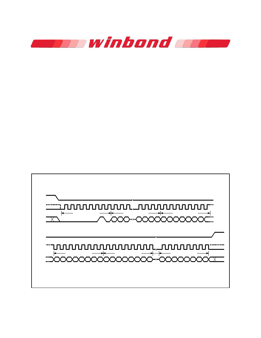
9.2.21
Page Program (02h)
The Page Program instruction allows from one byte to 256 bytes (a page) of data to be programmed at
previously erased (FFh) memory locations. A Write Enable instruction must be executed before the
device will accept the Page Program Instruction (Status Register bit WEL= 1). The instruction is initiated
by driving the /CS pin low then shifting the instruction code “02h” followed by a 24-bit address (A23-A0)
and at least one data byte, into the DI pin. The /CS pin must be held low for the entire length of the
instruction while data is being sent to the device. The Page Program instruction sequence is shown in
figure 19.
If an entire 256 byte page is to be programmed, the last address byte (the 8 least significant address bits)
should be set to 0. If the last address byte is not zero, and the number of clocks exceed the remaining
page length, the addressing will wrap to the beginning of the page. In some cases, less than 256 bytes (a
partial page) can be programmed without having any effect on other bytes within the same page. One
condition to perform a partial page program is that the number of clocks can not exceed the remaining
page length. If more than 256 bytes are sent to the device the addressing will wrap to the beginning of the
page and overwrite previously sent data.
As with the write and erase instructions, the /CS pin must be driven high after the eighth bit of the last
byte has been latched. If this is not done the Page Program instruction will not be executed. After /CS is
driven high, the self-timed Page Program instruction will commence for a time duration of tpp (See AC
Characteristics). While the Page Program cycle is in progress, the Read Status Register instruction may
still be accessed for checking the status of the BUSY bit. The BUSY bit is a 1 during the Page Program
cycle and becomes a 0 when the cycle is finished and the device is ready to accept other instructions
again. After the Page Program cycle has finished the Write Enable Latch (WEL) bit in the Status Register
is cleared to 0. The Page Program instruction will not be executed if the addressed page is protected by
the Block Protect (CMP, SEC, TB, BP2, BP1, and BP0) bits.
/CS
CLK
DI
(IO
0)
Mode 0
Mode 3
0
1
2
3
4
5
6
7
Instruction (02h)
8
9
10
28
29
30
39
24-Bit Address
23
22
21
3
2
1
*
/CS
CLK
40
DI
(IO
0)
41
42
43
44
45
46
47
Data Byte 2
48
49
50
52
53
54
55
20
72
51
39
7
6
5
4
3
2
1
0
31
0
32
33
34
35
36
37
38
Data Byte 1
7
6
5
4
3
2
1
*
Mode 0
Mode 3
Data Byte 3
20
73
20
74
20
75
20
76
20
77
20
78
20
79
0
Data Byte 256
*
7
6
5
4
3
2
1
0
*
7
6
5
4
3
2
1
0
*
= MSB
*
Figure 19. Page Program Instruction Sequence Diagram
相关PDF资料 |
PDF描述 |
|---|---|
| W25Q80BVSNIP | 8M X 1 SPI BUS SERIAL EEPROM, PDSO8 |
| W25X10AVDIAZ | 128K X 8 FLASH 2.7V PROM, PDIP8 |
| W25X16AVDAIG | 2M X 8 FLASH 2.7V PROM, PDIP8 |
| W25X16BVZPIG | 256K X 16 FLASH 2.7V PROM, PDSO8 |
| W25X20BLSNIG | 2M X 1 FLASH 2.7V PROM, PDSO8 |
相关代理商/技术参数 |
参数描述 |
|---|---|
| W25Q80BVZPAP | 制造商:WINBOND 制造商全称:Winbond 功能描述:8M-BIT SERIAL FLASH MEMORY WITH DUAL AND QUAD SPI |
| W25Q80BVZPIG | 功能描述:IC SPI FLASH 8MBIT 8WSON RoHS:是 类别:集成电路 (IC) >> 存储器 系列:SpiFlash® 标准包装:1,000 系列:- 格式 - 存储器:EEPROMs - 串行 存储器类型:EEPROM 存储容量:4K (512 x 8) 速度:400kHz 接口:I²C,2 线串口 电源电压:2.7 V ~ 5.5 V 工作温度:-40°C ~ 85°C 封装/外壳:8-SOIC(0.173",4.40mm 宽) 供应商设备封装:8-MFP 包装:带卷 (TR) |
| W25Q80BVZPIG TR | 制造商:Winbond Electronics Corp 功能描述:IC FLASH 8MBIT 104MHZ 8WSON |
| W25Q80BVZPIP | 制造商:WINBOND 制造商全称:Winbond 功能描述:8M-BIT SERIAL FLASH MEMORY WITH DUAL AND QUAD SPI |
| W25Q80BW | 制造商:WINBOND 制造商全称:Winbond 功能描述:1.8V 8M-BIT SERIAL FLASH MEMORY WITH DUAL AND QUAD SPI |
发布紧急采购,3分钟左右您将得到回复。