- 您现在的位置:买卖IC网 > PDF目录68457 > W3H32M72E-667SB2M (MICROSEMI CORP-PMG MICROELECTRONICS) 32M X 72 DDR DRAM, 0.65 ns, PBGA208 PDF资料下载
参数资料
| 型号: | W3H32M72E-667SB2M |
| 厂商: | MICROSEMI CORP-PMG MICROELECTRONICS |
| 元件分类: | DRAM |
| 英文描述: | 32M X 72 DDR DRAM, 0.65 ns, PBGA208 |
| 封装: | 16 X 20 MM, 1 MM PITCH, PLASTIC, BGA-208 |
| 文件页数: | 4/25页 |
| 文件大小: | 1062K |
| 代理商: | W3H32M72E-667SB2M |
W3H32M72E-XSB2X
November 2010 2010 Microsemi Corporation. All rights reserved.
12
Microsemi Corporation (602) 437-1520 www.whiteedc.com
Rev. 3
www.microsemi.com
Microsemi Corporation reserves the right to change products or specications without notice.
the EMR. The ODT feature and ODT input ball are only used during
active, active power-down (both fast-exit and slow-exit modes), and
precharge power-down modes of operation. ODT must be turned
off prior to entering self refresh. During power-up and initialization
of the DDR2 SDRAM, ODT should be disabled until issuing the
EMR command to enable the ODT feature, at which point the ODT
ball will determine the RTT(EFF) value. Any time the EMR enables
the ODT function, ODT may not be driven HIGH until eight clocks
after the EMR has been enabled. See “ODT Timing” section for
ODT timing diagrams.
POSTED CAS ADDITIVE LATENCY (AL)
Posted CAS additive latency (AL) is supported to make the
command and data bus efcient for sustainable bandwidths in
DDR2 SDRAM. Bits E3–E5 dene the value of AL, as shown in
Figure 7. Bits E3–E5 allow the user to program the DDR2 SDRAM
with an inverse AL of 0, 1, 2, 3, or 4 clocks. Reserved states should
not be used as unknown operation or incompatibility with future
versions may result.
In this operation, the DDR2 SDRAM allows a READ or WRITE
command to be issued prior to tRCD (MIN) with the requirement
that AL ≤ tRCD (MIN). A typical application using this feature would
set AL = tRCD (MIN) - 1x tCK. The READ or WRITE command is
held for the time of the AL before it is issued internally to the DDR2
SDRAM device. RL is controlled by the sum of AL and CL; RL =
AL+CL. Write latency (WL) is equal to RL minus one clock; WL =
AL + CL - 1 x tCK.
EXTENDED MODE REGISTER 2
The extended mode register 2 (EMR2) controls functions beyond
those controlled by the mode register. Currently all bits in EMR2
are reserved, as shown in Figure 8. The EMR2 is programmed
via the LM command and will retain the stored information until it
is programmed again or the device loses power. Reprogramming
the EMR will not alter the contents of the memory array, provided
it is performed correctly.
EMR2 must be loaded when all banks are idle and no bursts are
in progress, and the controller must wait the specied time tMRD
before initiating any subsequent operation. Violating either of these
requirements could result in unspecied operation.
EXTENDED MODE REGISTER 3
The extended mode register 3 (EMR3) controls functions beyond
those controlled by the mode register. Currently, all bits in EMR3
are reserved, as shown in Figure 9. The EMR3 is programmed
via the LM command and will retain the stored information until it
is programmed again or the device loses power. Reprogramming
the EMR will not alter the contents of the memory array, provided
it is performed correctly.
EMR3 must be loaded when all banks are idle and no bursts are
in progress, and the controller must wait the specied time tMRD
before initiating any subsequent operation. Violating either of these
requirements could result in unspecied operation.
COMMAND TRUTH TABLES
The following tables provide a quick reference of DDR2 SDRAM
available commands, including CKE power-down modes, and
bank-to-bank commands.
DESELECT
The DESELECT function (CS# HIGH) prevents new commands
from being executed by the DDR2 SDRAM. The DDR2 SDRAM
is effectively deselected. Operations already in progress are not
affected.
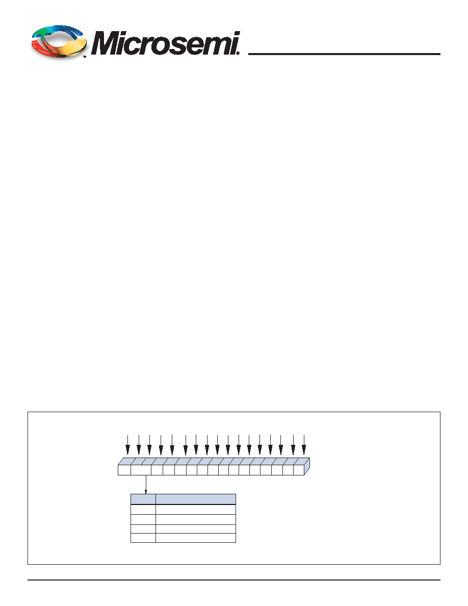
FIGURE 9 – EXTENDED MODE REGISTER 3 (EMR3) DEFINITION
A9
A7 A 6 A5 A4 A3
A8
A2
A1 A0
Extended Mo de
Register (Ex)
Address Bus
97
6
5
4
3
82
1
0
A10
A12 A11
BA0
BA1
BA2
10
11
12
13
14
1
16
5
A13
0
1
0
1
Mode Register Definition
Mo de Register (MR)
Extended Mo de Register (EMR)
Extended Mo de Register (EMR2)
Extended Mo de Register (EMR3)
M15
0
1
M14
EMR3
01
Note: 1. E13 (A13)-E0 (A0) are reserved for future use and must be programmed to "0." A13 is not used in this device.
相关PDF资料 |
PDF描述 |
|---|---|
| W3H32M72E-667SBC | 32M X 72 DDR DRAM, 0.65 ns, PBGA208 |
| W3H64M16E-400BC | 64M X 16 DDR DRAM, 0.6 ns, PBGA79 |
| W3H64M64E-400SBC | 64M X 64 DDR DRAM, 0.6 ns, PBGA208 |
| W3H64M72E-400ESI | 64M X 72 DDR DRAM, 0.6 ns, PBGA208 |
| W3H64M72E-400ESI | 64M X 72 DDR DRAM, 0.6 ns, PBGA208 |
相关代理商/技术参数 |
参数描述 |
|---|---|
| W3H32M72E-667SB2M/T/R | 制造商:Microsemi Corporation 功能描述:PBGA,32M X72,DDR2 SDRAM, 1.8V - Tape and Reel |
| W3H32M72E-667SBC | 制造商:Microsemi Corporation 功能描述:32M X 72 DDR2, 1.8V, 667MHZ, 208PBGA COMMERICAL TEMP. - Bulk |
| W3H32M72E-667SBI | 制造商:Microsemi Corporation 功能描述:32M X 72 DDR2, 1.8V, 667MHZ, 208PBGA INDUSTRIAL TEMP. - Bulk |
| W3H32M72E-667SBM | 制造商:PMG/Microsemi 功能描述: |
| W3H32M72E-ES | 制造商:WEDC 制造商全称:White Electronic Designs Corporation 功能描述:32M x 72 DDR2 SDRAM 208 PBGA Multi-Chip Package |
发布紧急采购,3分钟左右您将得到回复。