- 您现在的位置:买卖IC网 > PDF目录68457 > W3H32M72E-667SB2M (MICROSEMI CORP-PMG MICROELECTRONICS) 32M X 72 DDR DRAM, 0.65 ns, PBGA208 PDF资料下载
参数资料
| 型号: | W3H32M72E-667SB2M |
| 厂商: | MICROSEMI CORP-PMG MICROELECTRONICS |
| 元件分类: | DRAM |
| 英文描述: | 32M X 72 DDR DRAM, 0.65 ns, PBGA208 |
| 封装: | 16 X 20 MM, 1 MM PITCH, PLASTIC, BGA-208 |
| 文件页数: | 5/25页 |
| 文件大小: | 1062K |
| 代理商: | W3H32M72E-667SB2M |
W3H32M72E-XSB2X
November 2010 2010 Microsemi Corporation. All rights reserved.
13
Microsemi Corporation (602) 437-1520 www.whiteedc.com
Rev. 3
www.microsemi.com
Microsemi Corporation reserves the right to change products or specications without notice.
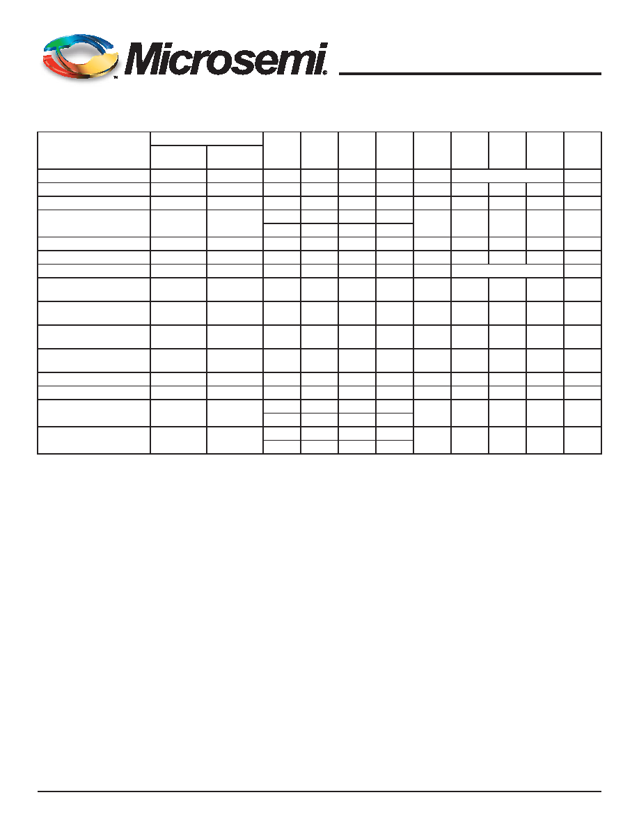
TABLE 3 – TRUTH TABLE - DDR2 COMMANDS
Function
CKE
CS#
RAS#
CAS#
WE#
BA1
BA0
A12
A11
A10
A9-A0
Notes
Previous
Cycle
Current Cycle
LOAD MODE
H
LLLL
BA
OP Code
2
REFRESH
H
L
H
XXXX
SELF-REFRESH Entry
H
L
H
XXXX
SELF-REFRESH Exit
LH
H
XXX
XXXX
7
L
HHH
Single bank precharge
HH
L
H
L
X
L
X
2
All banks PRECHARGE
HH
L
H
L
X
H
X
Bank activate
H
L
H
L
BA
Row Address
WRITE
HH
L
H
L
BA
Column
Address
L
Column
Address
2, 3
WRITE with auto precharge
HH
L
H
L
BA
Column
Address
H
Column
Address
2, 3
READ
H
LH
BA
Column
Address
L
Column
Address
2, 3
READ with auto precharge
H
LH
BA
Column
Address
H
Column
Address
2, 3
NO OPERATION
H
X
L
H
XXXX
Device DESELECT
H
X
H
XXXXXXX
POWER-DOWN entry
HL
H
XXX
XXXX
4
L
HHH
POWER-DOWN exit
LH
H
XXX
XXXX
4
L
HHH
Note: 1. All DDR2 SDRAM commands are dened by states of CS#, RAS#, CAS#, WE#, and CKE at the rising edge of the clock.
2. Bank addresses (BA) BA0–BA12 determine which bank is to be operated upon. BA during a LM command selects which mode register is programmed.
3. 3. Burst reads or writes at BL = 4 cannot be terminated or interrupted.
4. The power-down mode does not perform any REFRESH operations. The duration of power-down is therefore limited by the refresh requirements outlined in the AC parametric section.
5. The state of ODT does not affect the states described in this table. The ODT function is not available during self refresh. See “On-Die Termination (ODT)” for details.
6. “X” means “H or L” (but a dened logic level).
7. Self refresh exit is asynchronous.
NO OPERATION (NOP)
The NO OPERATION (NOP) command is used to instruct the
selected DDR2 SDRAM to perform a NOP (CS# is LOW; RAS#,
CAS#, and WE are HIGH). This prevents unwanted commands
from being registered during idle or wait states. Operations already
in progress are not affected.
LOAD MODE (LM)
The mode registers are loaded via inputs BA1–BA0, and A12–A0.
BA1–BA0 determine which mode register will be programmed.
See “Mode Register (MR)”. The LM command can only be issued
when all banks are idle, and a subsequent execute able command
cannot be issued until tMRD is met.
BANK/ROW ACTIVATION
ACTIVE COMMAND
The ACTIVE command is used to open (or activate) a row in a
particular bank for a subsequent access. The value on the BA1–
BA0 inputs selects the bank, and the address provided on inputs
A12–A0 selects the row. This row remains active (or open) for
accesses until a PRECHARGE command is issued to that bank. A
PRECHARGE command must be issued before opening a different
row in the same bank.
ACTIVE OPERATION
Before any READ or WRITE commands can be issued to a
bank within the DDR2 SDRAM, a row in that bank must be
相关PDF资料 |
PDF描述 |
|---|---|
| W3H32M72E-667SBC | 32M X 72 DDR DRAM, 0.65 ns, PBGA208 |
| W3H64M16E-400BC | 64M X 16 DDR DRAM, 0.6 ns, PBGA79 |
| W3H64M64E-400SBC | 64M X 64 DDR DRAM, 0.6 ns, PBGA208 |
| W3H64M72E-400ESI | 64M X 72 DDR DRAM, 0.6 ns, PBGA208 |
| W3H64M72E-400ESI | 64M X 72 DDR DRAM, 0.6 ns, PBGA208 |
相关代理商/技术参数 |
参数描述 |
|---|---|
| W3H32M72E-667SB2M/T/R | 制造商:Microsemi Corporation 功能描述:PBGA,32M X72,DDR2 SDRAM, 1.8V - Tape and Reel |
| W3H32M72E-667SBC | 制造商:Microsemi Corporation 功能描述:32M X 72 DDR2, 1.8V, 667MHZ, 208PBGA COMMERICAL TEMP. - Bulk |
| W3H32M72E-667SBI | 制造商:Microsemi Corporation 功能描述:32M X 72 DDR2, 1.8V, 667MHZ, 208PBGA INDUSTRIAL TEMP. - Bulk |
| W3H32M72E-667SBM | 制造商:PMG/Microsemi 功能描述: |
| W3H32M72E-ES | 制造商:WEDC 制造商全称:White Electronic Designs Corporation 功能描述:32M x 72 DDR2 SDRAM 208 PBGA Multi-Chip Package |
发布紧急采购,3分钟左右您将得到回复。