参数资料
| 型号: | XA3S400A-4FGG400I |
| 厂商: | Xilinx Inc |
| 文件页数: | 37/57页 |
| 文件大小: | 0K |
| 描述: | IC FPGA SPARTAN-3A 400K 400-FBGA |
| 产品培训模块: | Extended Spartan 3A FPGA Family |
| 标准包装: | 60 |
| 系列: | Spartan®-3A XA |
| LAB/CLB数: | 896 |
| 逻辑元件/单元数: | 8064 |
| RAM 位总计: | 368640 |
| 输入/输出数: | 311 |
| 门数: | 400000 |
| 电源电压: | 1.14 V ~ 1.26 V |
| 安装类型: | 表面贴装 |
| 工作温度: | -40°C ~ 100°C |
| 封装/外壳: | 400-BGA |
| 供应商设备封装: | 400-FBGA(21x21) |
第1页第2页第3页第4页第5页第6页第7页第8页第9页第10页第11页第12页第13页第14页第15页第16页第17页第18页第19页第20页第21页第22页第23页第24页第25页第26页第27页第28页第29页第30页第31页第32页第33页第34页第35页第36页当前第37页第38页第39页第40页第41页第42页第43页第44页第45页第46页第47页第48页第49页第50页第51页第52页第53页第54页第55页第56页第57页
XA Spartan-3A Automotive FPGA Family Data Sheet
DS681 (v2.0) April 22, 2011
Product Specification
42
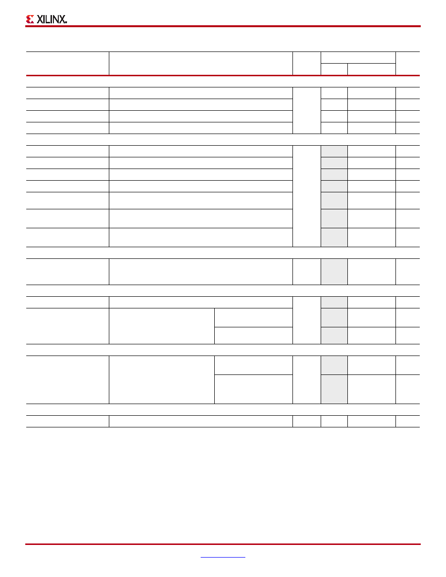
Table 36: Switching Characteristics for the DLL
Symbol
Description
Device
Speed Grade: -4
Units
Min
Max
Output Frequency Ranges
CLKOUT_FREQ_CLK0
Frequency for the CLK0 and CLK180 outputs
All
5
250
MHz
CLKOUT_FREQ_CLK90
Frequency for the CLK90 and CLK270 outputs
5
200
MHz
CLKOUT_FREQ_2X
Frequency for the CLK2X and CLK2X180 outputs
10
334
MHz
CLKOUT_FREQ_DV
Frequency for the CLKDV output
0.3125
166
MHz
Output Clock Jitter(2,3,4)
CLKOUT_PER_JITT_0
Period jitter at the CLK0 output
All
–±100
ps
CLKOUT_PER_JITT_90
Period jitter at the CLK90 output
–±150
ps
CLKOUT_PER_JITT_180
Period jitter at the CLK180 output
–±150
ps
CLKOUT_PER_JITT_270
Period jitter at the CLK270 output
–±150
ps
CLKOUT_PER_JITT_2X
Period jitter at the CLK2X and CLK2X180 outputs
–
±[0.5% of CLKIN
period + 100]
ps
CLKOUT_PER_JITT_DV1
Period jitter at the CLKDV output when performing integer
division
–±150
ps
CLKOUT_PER_JITT_DV2
Period jitter at the CLKDV output when performing non-integer
division
–
±[0.5% of CLKIN
period + 100]
ps
Duty Cycle(4)
CLKOUT_DUTY_CYCLE_
DLL
Duty cycle variation for the CLK0, CLK90, CLK180, CLK270,
CLK2X, CLK2X180, and CLKDV outputs, including the
BUFGMUX and clock tree duty-cycle distortion
All
–
±[1% of CLKIN
period + 350]
ps
Phase Alignment(4)
CLKIN_CLKFB_PHASE
Phase offset between the CLKIN and CLKFB inputs
All
–±150
ps
CLKOUT_PHASE_DLL
Phase offset between DLL outputs
CLK0 to CLK2X
(not CLK2X180)
–
±[1% of CLKIN
period + 100]
ps
All others
–
±[1% of CLKIN
period + 150]
ps
Lock Time
LOCK_DLL(3)
When using the DLL alone: The
time from deassertion at the DCM’s
Reset input to the rising transition
at its LOCKED output. When the
DCM is locked, the CLKIN and
CLKFB signals are in phase
5 MHz
F
CLKIN
15 MHz
All
–5
ms
FCLKIN 15 MHz
–600
s
Delay Lines
DCM_DELAY_STEP(5)
Finest delay resolution, averaged over all steps
All
15
35
ps
Notes:
1.
2.
Indicates the maximum amount of output jitter that the DCM adds to the jitter on the CLKIN input.
3.
For optimal jitter tolerance and faster lock time, use the CLKIN_PERIOD attribute.
4.
Some jitter and duty-cycle specifications include 1% of input clock period or 0.01 UI. For example, the data sheet specifies a maximum jitter
of “±[1% of CLKIN period + 150]”. Assume the CLKIN frequency is 100 MHz. The equivalent CLKIN period is 10 ns and 1% of 10 ns is 0.1 ns
or 100 ps. According to the data sheet, the maximum jitter is ±[100 ps + 150 ps] = ±250ps.
5.
The typical delay step size is 23 ps.
相关PDF资料 |
PDF描述 |
|---|---|
| XC6SLX25T-3CSG324C | IC FPGA SPARTAN 6 24K 324CSGBGA |
| XCV50E-6PQ240C | IC FPGA 1.8V C-TEMP 240-PQFP |
| ABB50DHBS | CONN EDGECARD 100PS R/A .050 SLD |
| XCV50E-6FG256C | IC FPGA 1.8V C-TEMP 256-FBGA |
| XC6SLX25-L1CSG324I | IC FPGA SPARTAN 6 24K 324CSGBGA |
相关代理商/技术参数 |
参数描述 |
|---|---|
| XA3S400A-4FGG400Q | 功能描述:IC FPGA SPARTAN-3A 400K 400-FBGA RoHS:是 类别:集成电路 (IC) >> 嵌入式 - FPGA(现场可编程门阵列) 系列:Spartan®-3A XA 标准包装:40 系列:Spartan® 6 LX LAB/CLB数:3411 逻辑元件/单元数:43661 RAM 位总计:2138112 输入/输出数:358 门数:- 电源电压:1.14 V ~ 1.26 V 安装类型:表面贴装 工作温度:-40°C ~ 100°C 封装/外壳:676-BGA 供应商设备封装:676-FBGA(27x27) |
| XA3S400A-4FTG256I | 功能描述:IC FPGA SPARTAN-3A 400K 256FTBGA RoHS:是 类别:集成电路 (IC) >> 嵌入式 - FPGA(现场可编程门阵列) 系列:Spartan®-3A XA 标准包装:40 系列:Spartan® 6 LX LAB/CLB数:3411 逻辑元件/单元数:43661 RAM 位总计:2138112 输入/输出数:358 门数:- 电源电压:1.14 V ~ 1.26 V 安装类型:表面贴装 工作温度:-40°C ~ 100°C 封装/外壳:676-BGA 供应商设备封装:676-FBGA(27x27) |
| XA3S400A-4FTG256Q | 功能描述:IC FPGA SPARTAN-3A 400K 256FTBGA RoHS:是 类别:集成电路 (IC) >> 嵌入式 - FPGA(现场可编程门阵列) 系列:Spartan®-3A XA 标准包装:40 系列:Spartan® 6 LX LAB/CLB数:3411 逻辑元件/单元数:43661 RAM 位总计:2138112 输入/输出数:358 门数:- 电源电压:1.14 V ~ 1.26 V 安装类型:表面贴装 工作温度:-40°C ~ 100°C 封装/外壳:676-BGA 供应商设备封装:676-FBGA(27x27) |
| XA3S500E | 制造商:XILINX 制造商全称:XILINX 功能描述:XA Spartan-3E Automotive FPGA Family Data Sheet |
| XA3S500E-4CPG132I | 功能描述:IC FPGA SPARTAN-3E 500K 132CSBGA RoHS:是 类别:集成电路 (IC) >> 嵌入式 - FPGA(现场可编程门阵列) 系列:Spartan®-3E XA 标准包装:40 系列:Spartan® 6 LX LAB/CLB数:3411 逻辑元件/单元数:43661 RAM 位总计:2138112 输入/输出数:358 门数:- 电源电压:1.14 V ~ 1.26 V 安装类型:表面贴装 工作温度:-40°C ~ 100°C 封装/外壳:676-BGA 供应商设备封装:676-FBGA(27x27) |
发布紧急采购,3分钟左右您将得到回复。