- 您现在的位置:买卖IC网 > PDF目录21989 > XC2S50-5PQG208C (Xilinx Inc)IC SPARTAN-II FPGA 50K 208-PQFP PDF资料下载
参数资料
| 型号: | XC2S50-5PQG208C |
| 厂商: | Xilinx Inc |
| 文件页数: | 20/99页 |
| 文件大小: | 0K |
| 描述: | IC SPARTAN-II FPGA 50K 208-PQFP |
| 标准包装: | 24 |
| 系列: | Spartan®-II |
| LAB/CLB数: | 384 |
| 逻辑元件/单元数: | 1728 |
| RAM 位总计: | 32768 |
| 输入/输出数: | 140 |
| 门数: | 50000 |
| 电源电压: | 2.375 V ~ 2.625 V |
| 安装类型: | 表面贴装 |
| 工作温度: | 0°C ~ 85°C |
| 封装/外壳: | 208-BFQFP |
| 供应商设备封装: | 208-PQFP(28x28) |
| 产品目录页面: | 599 (CN2011-ZH PDF) |
| 其它名称: | 122-1320 |
第1页第2页第3页第4页第5页第6页第7页第8页第9页第10页第11页第12页第13页第14页第15页第16页第17页第18页第19页当前第20页第21页第22页第23页第24页第25页第26页第27页第28页第29页第30页第31页第32页第33页第34页第35页第36页第37页第38页第39页第40页第41页第42页第43页第44页第45页第46页第47页第48页第49页第50页第51页第52页第53页第54页第55页第56页第57页第58页第59页第60页第61页第62页第63页第64页第65页第66页第67页第68页第69页第70页第71页第72页第73页第74页第75页第76页第77页第78页第79页第80页第81页第82页第83页第84页第85页第86页第87页第88页第89页第90页第91页第92页第93页第94页第95页第96页第97页第98页第99页
Spartan-II FPGA Family: Functional Description
DS001-2 (v2.8) June 13, 2008
Module 2 of 4
Product Specification
27
R
Design Considerations
This section contains more detailed design information on
the following features:
Delay-Locked Loop . . . see page 27
Block RAM . . . see page 32
Versatile I/O . . . see page 36
Using Delay-Locked Loops
The Spartan-II FPGA family provides up to four fully digital
dedicated on-chip Delay-Locked Loop (DLL) circuits which
provide zero propagation delay, low clock skew between
output clock signals distributed throughout the device, and
advanced clock domain control. These dedicated DLLs can
be used to implement several circuits that improve and
simplify system level design.
Introduction
Quality on-chip clock distribution is important. Clock skew
and clock delay impact device performance and the task of
managing clock skew and clock delay with conventional
clock trees becomes more difficult in large devices. The
Spartan-II family of devices resolve this potential problem
by providing up to four fully digital dedicated on-chip
Delay-Locked Loop (DLL) circuits which provide zero
propagation delay and low clock skew between output clock
signals distributed throughout the device.
Each DLL can drive up to two global clock routing networks
within the device. The global clock distribution network
minimizes clock skews due to loading differences. By
monitoring a sample of the DLL output clock, the DLL can
compensate for the delay on the routing network, effectively
eliminating the delay from the external input port to the
individual clock loads within the device.
In addition to providing zero delay with respect to a user
source clock, the DLL can provide multiple phases of the
source clock. The DLL can also act as a clock doubler or it
can divide the user source clock by up to 16.
Clock multiplication gives the designer a number of design
alternatives. For instance, a 50 MHz source clock doubled
by the DLL can drive an FPGA design operating at
100 MHz. This technique can simplify board design
because the clock path on the board no longer distributes
such a high-speed signal. A multiplied clock also provides
designers the option of time-domain-multiplexing, using one
circuit twice per clock cycle, consuming less area than two
copies of the same circuit.
The DLL can also act as a clock mirror. By driving the DLL
output off-chip and then back in again, the DLL can be used
to de-skew a board level clock between multiple devices.
In order to guarantee the system clock establishes prior to
the device "waking up," the DLL can delay the completion of
the device configuration process until after the DLL
achieves lock.
By taking advantage of the DLL to remove on-chip clock
delay, the designer can greatly simplify and improve system
level design involving high-fanout, high-performance
clocks.
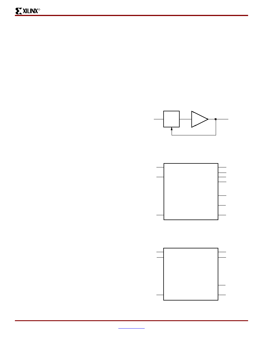
Library DLL Primitives
Figure 22 shows the simplified Xilinx library DLL macro,
BUFGDLL. This macro delivers a quick and efficient way to
provide a system clock with zero propagation delay
two library DLL primitives. These primitives provide access
to the complete set of DLL features when implementing
more complex applications.
Figure 22: Simplified DLL Macro BUFGDLL
Figure 23: Standard DLL Primitive CLKDLL
Figure 24: High-Frequency DLL Primitive CLKDLLHF
0 ns
DS001_22_032300
O
I
CLK0
CLK90
CLK180
CLK270
CLKIN
DS001_23_032300
CLKDLL
RST
CLKFB
CLK2X
CLKDV
LOCKED
CLK0
CLK180
CLKDV
LOCKED
CLKIN
DS001_24_032300
CLKDLLHF
RST
CLKFB
相关PDF资料 |
PDF描述 |
|---|---|
| FMC13DRYN-S734 | CONN EDGECARD 26POS DIP .100 SLD |
| TACR336M010RTA | CAP TANT 33UF 10V 20% 0805 |
| XC3S250E-4VQG100C | IC SPARTAN-3E FPGA 250K 100VQFP |
| FMC13DRYH-S734 | CONN EDGECARD 26POS DIP .100 SLD |
| XC3S100E-4TQG144I | IC FPGA SPARTAN-3E 100K 144-TQFP |
相关代理商/技术参数 |
参数描述 |
|---|---|
| XC2S50-5PQG208I | 制造商:Xilinx 功能描述:FPGA SPARTAN-II 50K GATES 1728 CELLS 263MHZ 2.5V 208PQFP - Trays |
| XC2S50-5TQ144C | 功能描述:IC FPGA 2.5V 384 CLB'S 144-TQFP RoHS:否 类别:集成电路 (IC) >> 嵌入式 - FPGA(现场可编程门阵列) 系列:Spartan®-II 标准包装:40 系列:Spartan® 6 LX LAB/CLB数:3411 逻辑元件/单元数:43661 RAM 位总计:2138112 输入/输出数:358 门数:- 电源电压:1.14 V ~ 1.26 V 安装类型:表面贴装 工作温度:-40°C ~ 100°C 封装/外壳:676-BGA 供应商设备封装:676-FBGA(27x27) |
| XC2S50-5TQ144C-ES | 制造商:Xilinx 功能描述:2S50-5TQ144C-ES |
| XC2S50-5TQ144I | 功能描述:IC FPGA 2.5V I-TEMP 144-TQFP RoHS:否 类别:集成电路 (IC) >> 嵌入式 - FPGA(现场可编程门阵列) 系列:Spartan®-II 标准包装:40 系列:Spartan® 6 LX LAB/CLB数:3411 逻辑元件/单元数:43661 RAM 位总计:2138112 输入/输出数:358 门数:- 电源电压:1.14 V ~ 1.26 V 安装类型:表面贴装 工作温度:-40°C ~ 100°C 封装/外壳:676-BGA 供应商设备封装:676-FBGA(27x27) |
| XC2S50-5TQG144C | 功能描述:IC SPARTAN-II FPGA 50K 144-TQFP RoHS:是 类别:集成电路 (IC) >> 嵌入式 - FPGA(现场可编程门阵列) 系列:Spartan®-II 标准包装:60 系列:XP LAB/CLB数:- 逻辑元件/单元数:10000 RAM 位总计:221184 输入/输出数:244 门数:- 电源电压:1.71 V ~ 3.465 V 安装类型:表面贴装 工作温度:0°C ~ 85°C 封装/外壳:388-BBGA 供应商设备封装:388-FPBGA(23x23) 其它名称:220-1241 |
发布紧急采购,3分钟左右您将得到回复。