- 您现在的位置:买卖IC网 > PDF目录21989 > XC2S50-5PQG208C (Xilinx Inc)IC SPARTAN-II FPGA 50K 208-PQFP PDF资料下载
参数资料
| 型号: | XC2S50-5PQG208C |
| 厂商: | Xilinx Inc |
| 文件页数: | 59/99页 |
| 文件大小: | 0K |
| 描述: | IC SPARTAN-II FPGA 50K 208-PQFP |
| 标准包装: | 24 |
| 系列: | Spartan®-II |
| LAB/CLB数: | 384 |
| 逻辑元件/单元数: | 1728 |
| RAM 位总计: | 32768 |
| 输入/输出数: | 140 |
| 门数: | 50000 |
| 电源电压: | 2.375 V ~ 2.625 V |
| 安装类型: | 表面贴装 |
| 工作温度: | 0°C ~ 85°C |
| 封装/外壳: | 208-BFQFP |
| 供应商设备封装: | 208-PQFP(28x28) |
| 产品目录页面: | 599 (CN2011-ZH PDF) |
| 其它名称: | 122-1320 |
第1页第2页第3页第4页第5页第6页第7页第8页第9页第10页第11页第12页第13页第14页第15页第16页第17页第18页第19页第20页第21页第22页第23页第24页第25页第26页第27页第28页第29页第30页第31页第32页第33页第34页第35页第36页第37页第38页第39页第40页第41页第42页第43页第44页第45页第46页第47页第48页第49页第50页第51页第52页第53页第54页第55页第56页第57页第58页当前第59页第60页第61页第62页第63页第64页第65页第66页第67页第68页第69页第70页第71页第72页第73页第74页第75页第76页第77页第78页第79页第80页第81页第82页第83页第84页第85页第86页第87页第88页第89页第90页第91页第92页第93页第94页第95页第96页第97页第98页第99页
Spartan-II FPGA Family: DC and Switching Characteristics
DS001-3 (v2.8) June 13, 2008
Module 3 of 4
Product Specification
62
R
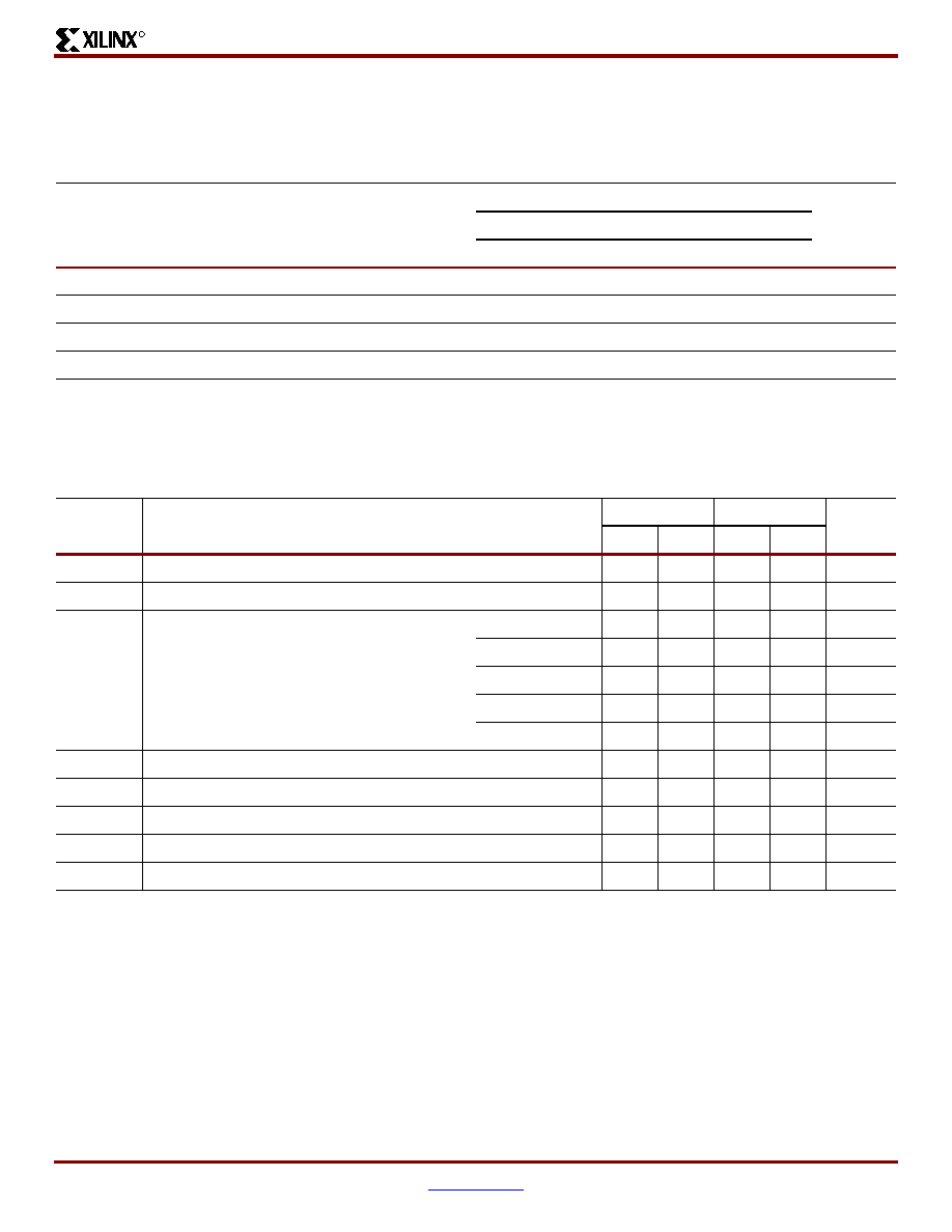
DLL Timing Parameters
All devices are 100 percent functionally tested. Because of
the difficulty in directly measuring many internal timing
parameters, those parameters are derived from benchmark
timing patterns. The following guidelines reflect worst-case
values across the recommended operating conditions.
DLL Clock Tolerance, Jitter, and Phase Information
All DLL output jitter and phase specifications were
determined through statistical measurement at the package
pins using a clock mirror configuration and matched drivers.
Figure 52, page 63, provides definitions for various
parameters in the table below.
Symbol
Description
Speed Grade
Units
-6
-5
Min
Max
Min
Max
FCLKINHF
Input clock frequency (CLKDLLHF)
60
200
60
180
MHz
FCLKINLF
Input clock frequency (CLKDLL)
25
100
25
90
MHz
TDLLPWHF
Input clock pulse width (CLKDLLHF)
2.0
-
2.4
-
ns
TDLLPWLF
Input clock pulse width (CLKDLL)
2.5
-
3.0
-
ns
Symbol
Description
F
CLKIN
CLKDLLHF
CLKDLL
Units
Min
Max
Min
Max
TIPTOL
Input clock period tolerance
-
1.0
-
1.0
ns
TIJITCC
Input clock jitter tolerance (cycle-to-cycle)
-
±150
-
±300
ps
TLOCK
Time required for DLL to acquire lock
> 60 MHz
-
20
-
20
μs
50-60 MHz
-
25
μs
40-50 MHz
-
50
μs
30-40 MHz
-
90
μs
25-30 MHz
-
120
μs
TOJITCC
Output jitter (cycle-to-cycle) for any DLL clock output(1)
-
±60
-
±60
ps
TPHIO
Phase offset between CLKIN and CLKO(2)
-
±100
-
±100
ps
TPHOO
Phase offset between clock outputs on the DLL(3)
-
±140
-
±140
ps
TPHIOM
Maximum phase difference between CLKIN and CLKO(4)
-
±160
-
±160
ps
TPHOOM
Maximum phase difference between clock outputs on the DLL(5)
-
±200
-
±200
ps
Notes:
1.
Output Jitter is cycle-to-cycle jitter measured on the DLL output clock, excluding input clock jitter.
2.
Phase Offset between CLKIN and CLKO is the worst-case fixed time difference between rising edges of CLKIN and CLKO,
excluding output jitter and input clock jitter.
3.
Phase Offset between Clock Outputs on the DLL is the worst-case fixed time difference between rising edges of any two DLL
outputs, excluding Output Jitter and input clock jitter.
4.
Maximum Phase Difference between CLKIN an CLKO is the sum of Output Jitter and Phase Offset between CLKIN and CLKO,
or the greatest difference between CLKIN and CLKO rising edges due to DLL alone (excluding input clock jitter).
5.
Maximum Phase Difference between Clock Outputs on the DLL is the sum of Output JItter and Phase Offset between any DLL
clock outputs, or the greatest difference between any two DLL output rising edges due to DLL alone (excluding input clock jitter).
相关PDF资料 |
PDF描述 |
|---|---|
| FMC13DRYN-S734 | CONN EDGECARD 26POS DIP .100 SLD |
| TACR336M010RTA | CAP TANT 33UF 10V 20% 0805 |
| XC3S250E-4VQG100C | IC SPARTAN-3E FPGA 250K 100VQFP |
| FMC13DRYH-S734 | CONN EDGECARD 26POS DIP .100 SLD |
| XC3S100E-4TQG144I | IC FPGA SPARTAN-3E 100K 144-TQFP |
相关代理商/技术参数 |
参数描述 |
|---|---|
| XC2S50-5PQG208I | 制造商:Xilinx 功能描述:FPGA SPARTAN-II 50K GATES 1728 CELLS 263MHZ 2.5V 208PQFP - Trays |
| XC2S50-5TQ144C | 功能描述:IC FPGA 2.5V 384 CLB'S 144-TQFP RoHS:否 类别:集成电路 (IC) >> 嵌入式 - FPGA(现场可编程门阵列) 系列:Spartan®-II 标准包装:40 系列:Spartan® 6 LX LAB/CLB数:3411 逻辑元件/单元数:43661 RAM 位总计:2138112 输入/输出数:358 门数:- 电源电压:1.14 V ~ 1.26 V 安装类型:表面贴装 工作温度:-40°C ~ 100°C 封装/外壳:676-BGA 供应商设备封装:676-FBGA(27x27) |
| XC2S50-5TQ144C-ES | 制造商:Xilinx 功能描述:2S50-5TQ144C-ES |
| XC2S50-5TQ144I | 功能描述:IC FPGA 2.5V I-TEMP 144-TQFP RoHS:否 类别:集成电路 (IC) >> 嵌入式 - FPGA(现场可编程门阵列) 系列:Spartan®-II 标准包装:40 系列:Spartan® 6 LX LAB/CLB数:3411 逻辑元件/单元数:43661 RAM 位总计:2138112 输入/输出数:358 门数:- 电源电压:1.14 V ~ 1.26 V 安装类型:表面贴装 工作温度:-40°C ~ 100°C 封装/外壳:676-BGA 供应商设备封装:676-FBGA(27x27) |
| XC2S50-5TQG144C | 功能描述:IC SPARTAN-II FPGA 50K 144-TQFP RoHS:是 类别:集成电路 (IC) >> 嵌入式 - FPGA(现场可编程门阵列) 系列:Spartan®-II 标准包装:60 系列:XP LAB/CLB数:- 逻辑元件/单元数:10000 RAM 位总计:221184 输入/输出数:244 门数:- 电源电压:1.71 V ~ 3.465 V 安装类型:表面贴装 工作温度:0°C ~ 85°C 封装/外壳:388-BBGA 供应商设备封装:388-FPBGA(23x23) 其它名称:220-1241 |
发布紧急采购,3分钟左右您将得到回复。