参数资料
| 型号: | XC2V40-4FG256I |
| 厂商: | Xilinx Inc |
| 文件页数: | 263/318页 |
| 文件大小: | 0K |
| 描述: | IC FPGA VIRTEX-II 256FGBGA |
| 产品变化通告: | FPGA Family Discontinuation 18/Apr/2011 |
| 标准包装: | 90 |
| 系列: | Virtex®-II |
| LAB/CLB数: | 64 |
| RAM 位总计: | 73728 |
| 输入/输出数: | 88 |
| 门数: | 40000 |
| 电源电压: | 1.425 V ~ 1.575 V |
| 安装类型: | 表面贴装 |
| 工作温度: | -40°C ~ 100°C |
| 封装/外壳: | 256-BGA |
| 供应商设备封装: | 256-FBGA(17x17) |
第1页第2页第3页第4页第5页第6页第7页第8页第9页第10页第11页第12页第13页第14页第15页第16页第17页第18页第19页第20页第21页第22页第23页第24页第25页第26页第27页第28页第29页第30页第31页第32页第33页第34页第35页第36页第37页第38页第39页第40页第41页第42页第43页第44页第45页第46页第47页第48页第49页第50页第51页第52页第53页第54页第55页第56页第57页第58页第59页第60页第61页第62页第63页第64页第65页第66页第67页第68页第69页第70页第71页第72页第73页第74页第75页第76页第77页第78页第79页第80页第81页第82页第83页第84页第85页第86页第87页第88页第89页第90页第91页第92页第93页第94页第95页第96页第97页第98页第99页第100页第101页第102页第103页第104页第105页第106页第107页第108页第109页第110页第111页第112页第113页第114页第115页第116页第117页第118页第119页第120页第121页第122页第123页第124页第125页第126页第127页第128页第129页第130页第131页第132页第133页第134页第135页第136页第137页第138页第139页第140页第141页第142页第143页第144页第145页第146页第147页第148页第149页第150页第151页第152页第153页第154页第155页第156页第157页第158页第159页第160页第161页第162页第163页第164页第165页第166页第167页第168页第169页第170页第171页第172页第173页第174页第175页第176页第177页第178页第179页第180页第181页第182页第183页第184页第185页第186页第187页第188页第189页第190页第191页第192页第193页第194页第195页第196页第197页第198页第199页第200页第201页第202页第203页第204页第205页第206页第207页第208页第209页第210页第211页第212页第213页第214页第215页第216页第217页第218页第219页第220页第221页第222页第223页第224页第225页第226页第227页第228页第229页第230页第231页第232页第233页第234页第235页第236页第237页第238页第239页第240页第241页第242页第243页第244页第245页第246页第247页第248页第249页第250页第251页第252页第253页第254页第255页第256页第257页第258页第259页第260页第261页第262页当前第263页第264页第265页第266页第267页第268页第269页第270页第271页第272页第273页第274页第275页第276页第277页第278页第279页第280页第281页第282页第283页第284页第285页第286页第287页第288页第289页第290页第291页第292页第293页第294页第295页第296页第297页第298页第299页第300页第301页第302页第303页第304页第305页第306页第307页第308页第309页第310页第311页第312页第313页第314页第315页第316页第317页第318页
2000–2007 Xilinx, Inc. All rights reserved. XILINX, the Xilinx logo, the Brand Window, and other designated brands included herein are trademarks of Xilinx, Inc. All other
trademarks are the property of their respective owners.
DS031-3 (v3.5) November 5, 2007
Module 3 of 4
Product Specification
1
Virtex-II Electrical Characteristics
Virtex-II devices are provided in -6, -5, and -4 speed
grades, with -6 having the highest performance.
Virtex-II DC and AC characteristics are specified for both
commercial and industrial grades. Except the operating
temperature range or unless otherwise noted, all the DC
and AC electrical parameters are the same for a particular
speed grade (that is, the timing characteristics of a -4 speed
grade industrial device are the same as for a -4 speed grade
commercial device). However, only selected speed grades
and/or devices might be available in the industrial range.
All supply voltage and junction temperature specifications
are representative of worst-case conditions. The parame-
ters included are common to popular designs and typical
applications. Contact Xilinx for design considerations
requiring more detailed information.
All specifications are subject to change without notice.
Virtex-II DC Characteristics
4
Virtex-II Platform FPGAs:
DC and Switching Characteristics
DS031-3 (v3.5) November 5, 2007
Product Specification
R
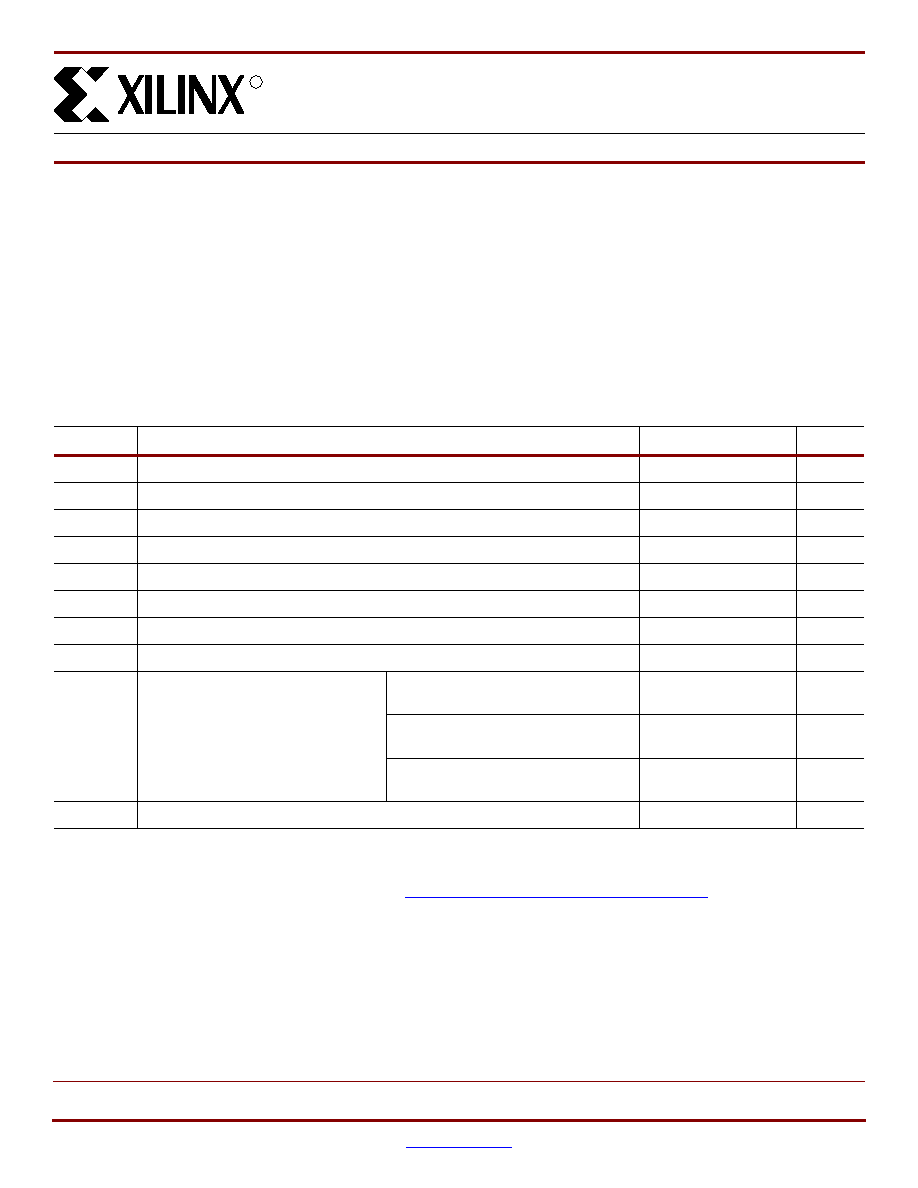
Table 1: Absolute Maximum Ratings
Symbol
Description(1)
Units
VCCINT
Internal supply voltage relative to GND
–0.5 to 1.65
V
VCCAUX
Auxiliary supply voltage relative to GND
–0.5 to 4.0
V
VCCO
Output drivers supply voltage relative to GND
–0.5 to 4.0
V
VBATT
Key memory battery backup supply
–0.5 to 4.0
V
VREF
Input reference voltage
–0.5 to VCCO + 0.5
V
VIN(3)
Input voltage relative to GND (user and dedicated I/Os)
–0.5 to VCCO + 0.5
V
VTS
Voltage applied to 3-state output (user and dedicated I/Os)
–0.5 to 4.0
V
TSTG
Storage temperature (ambient)
–65 to +150
°C
TSOL
Maximum soldering temperature(2)
All regular FF/BF flip-chip and
FG/BG/CS wire-bond packages
+220
°C
Pb-free FGG456, FGG676, BGG575,
and BGG728 wire-bond packages
+250
°C
Pb-free FGG256 and CSG144
wire-bond packages
+260
°C
TJ
Maximum junction temperature(2)
+125
°C
Notes:
1.
Stresses beyond those listed under Absolute Maximum Ratings might cause permanent damage to the device. These are stress ratings only, and
functional operation of the device at these or any other conditions beyond those listed under Operating Conditions is not implied. Exposure to
Absolute Maximum Ratings conditions for extended periods of time might affect device reliability.
2.
For soldering guidelines and thermal considerations, see the Device Packaging and Thermal Characteristics Guide information on the Xilinx
website.
3.
Inputs configured as PCI are fully PCI compliant. This statement takes precedence over any specification that would imply that the device is not PCI
compliant.
相关PDF资料 |
PDF描述 |
|---|---|
| XC2V40-5FGG256C | IC FPGA VIRTEX-II 40K 256-FBGA |
| XC2V40-4FGG256I | IC FPGA VIRTEX-II 40K 256-FBGA |
| 3341-32BULK | CONN JACKSOCKET M2.5/4-40 0.50" |
| DB53750-2 | DSUB DB INTERFACIAL SEAL |
| XC3S1400A-5FTG256C | IC FPGA SPARTAN3A 1400K 256FTBGA |
相关代理商/技术参数 |
参数描述 |
|---|---|
| XC2V40-4FG456C | 制造商:XILINX 制造商全称:XILINX 功能描述:Virtex-II Platform FPGAs: Complete Data Sheet |
| XC2V40-4FG456I | 制造商:XILINX 制造商全称:XILINX 功能描述:Virtex-II Platform FPGAs: Complete Data Sheet |
| XC2V40-4FGG256C | 功能描述:IC FPGA VIRTEX-II 40K 256-FBGA RoHS:是 类别:集成电路 (IC) >> 嵌入式 - FPGA(现场可编程门阵列) 系列:Virtex®-II 标准包装:40 系列:Spartan® 6 LX LAB/CLB数:3411 逻辑元件/单元数:43661 RAM 位总计:2138112 输入/输出数:358 门数:- 电源电压:1.14 V ~ 1.26 V 安装类型:表面贴装 工作温度:-40°C ~ 100°C 封装/外壳:676-BGA 供应商设备封装:676-FBGA(27x27) |
| XC2V40-4FGG256I | 功能描述:IC FPGA VIRTEX-II 40K 256-FBGA RoHS:是 类别:集成电路 (IC) >> 嵌入式 - FPGA(现场可编程门阵列) 系列:Virtex®-II 标准包装:40 系列:Spartan® 6 LX LAB/CLB数:3411 逻辑元件/单元数:43661 RAM 位总计:2138112 输入/输出数:358 门数:- 电源电压:1.14 V ~ 1.26 V 安装类型:表面贴装 工作温度:-40°C ~ 100°C 封装/外壳:676-BGA 供应商设备封装:676-FBGA(27x27) |
| XC2V40-5BF957C | 制造商:XILINX 制造商全称:XILINX 功能描述:Virtex-II 1.5V Field-Programmable Gate Arrays |
发布紧急采购,3分钟左右您将得到回复。