参数资料
| 型号: | XCV405E-7FG676C |
| 厂商: | Xilinx Inc |
| 文件页数: | 108/118页 |
| 文件大小: | 0K |
| 描述: | IC FPGA 1.8V C-TEMP 676-FBGA |
| 产品变化通告: | FPGA Family Discontinuation 18/Apr/2011 |
| 标准包装: | 1 |
| 系列: | Virtex®-E EM |
| LAB/CLB数: | 2400 |
| 逻辑元件/单元数: | 10800 |
| RAM 位总计: | 573440 |
| 输入/输出数: | 404 |
| 门数: | 129600 |
| 电源电压: | 1.71 V ~ 1.89 V |
| 安装类型: | 表面贴装 |
| 工作温度: | 0°C ~ 85°C |
| 封装/外壳: | 676-BGA |
| 供应商设备封装: | 676-FBGA(27x27) |
第1页第2页第3页第4页第5页第6页第7页第8页第9页第10页第11页第12页第13页第14页第15页第16页第17页第18页第19页第20页第21页第22页第23页第24页第25页第26页第27页第28页第29页第30页第31页第32页第33页第34页第35页第36页第37页第38页第39页第40页第41页第42页第43页第44页第45页第46页第47页第48页第49页第50页第51页第52页第53页第54页第55页第56页第57页第58页第59页第60页第61页第62页第63页第64页第65页第66页第67页第68页第69页第70页第71页第72页第73页第74页第75页第76页第77页第78页第79页第80页第81页第82页第83页第84页第85页第86页第87页第88页第89页第90页第91页第92页第93页第94页第95页第96页第97页第98页第99页第100页第101页第102页第103页第104页第105页第106页第107页当前第108页第109页第110页第111页第112页第113页第114页第115页第116页第117页第118页
Virtex-E 1.8 V Extended Memory Field Programmable Gate Arrays
DS025-2 (v3.0) March 21, 2014
Module 2 of 4
5
R
— OBSOLETE — OBSOLETE — OBSOLETE — OBSOLETE —
bined to create a 16 x 2-bit or 32 x 1-bit synchronous RAM,
or a 16 x 1-bit dual-port synchronous RAM.
The Virtex-E LUT can also provide a 16-bit shift register that
is ideal for capturing high-speed or burst-mode data. This
mode can also be used to store data in applications such as
Digital Signal Processing.
Storage Elements
The storage elements in the Virtex-E slice can be config-
ured either as edge-triggered D-type flip-flops or as
level-sensitive latches. The D inputs can be driven either by
the function generators within the slice or directly from slice
inputs, bypassing the function generators.
In addition to Clock and Clock Enable signals, each Slice
has synchronous set and reset signals (SR and BY). SR
forces a storage element into the initialization state speci-
fied for it in the configuration. BY forces it into the opposite
state. Alternatively, these signals can be configured to oper-
ate asynchronously. All of the control signals are indepen-
dently invertible, and are shared by the two flip-flops within
the slice.
Additional Logic
The F5 multiplexer in each slice combines the function gen-
erator outputs. This combination provides either a function
generator that can implement any 5-input function, a 4:1
multiplexer, or selected functions of up to nine inputs.
Similarly, the F6 multiplexer combines the outputs of all four
function generators in the CLB by selecting one of the
F5-multiplexer outputs. This permits the implementation of
any 6-input function, an 8:1 multiplexer, or selected func-
tions of up to 19 inputs.
Each CLB has four direct feedthrough paths, two per slice.
These paths provide extra data input lines or additional local
routing that does not consume logic resources.
Arithmetic Logic
Dedicated carry logic provides fast arithmetic carry capabil-
ity for high-speed arithmetic functions. The Virtex-E CLB
supports two separate carry chains, one per Slice. The
height of the carry chains is two bits per CLB.
The arithmetic logic includes an XOR gate that allows a
2-bit full adder to be implemented within a slice. In addition,
a dedicated AND gate improves the efficiency of multiplier
implementation.
The dedicated carry path can also be used to cascade func-
tion generators for implementing wide logic functions.
BUFTs
Each Virtex-E CLB contains two 3-state drivers (BUFTs)
that can drive on-chip busses. See "Dedicated Routing" on
page 7. Each Virtex-E BUFT has an independent 3-state
control pin and an independent input pin.
Block SelectRAM+ Memory
Virtex-E FPGAs incorporate large block SelectRAM memo-
ries. These complement the Distributed SelectRAM memo-
ries that provide shallow RAM structures implemented in
CLBs.
Block SelectRAM memory blocks are organized in columns,
starting at the left (column 0) and right outside edges and
inserted every four CLB columns (see notes for smaller
devices). Each memory block is four CLBs high, and each
memory column extends the full height of the chip, immedi-
ately adjacent (to the right, except for column 0) of the CLB
column locations indicated in Table 3.
Table 4 shows the amount of block SelectRAM memory that
is available in each Virtex-E device.
Each block SelectRAM cell, as illustrated in Figure 6, is a
fully synchronous dual-ported (True Dual Port) 4096-bit
RAM with independent control signals for each port. The
data widths of the two ports can be configured indepen-
dently, providing built-in bus-width conversion.
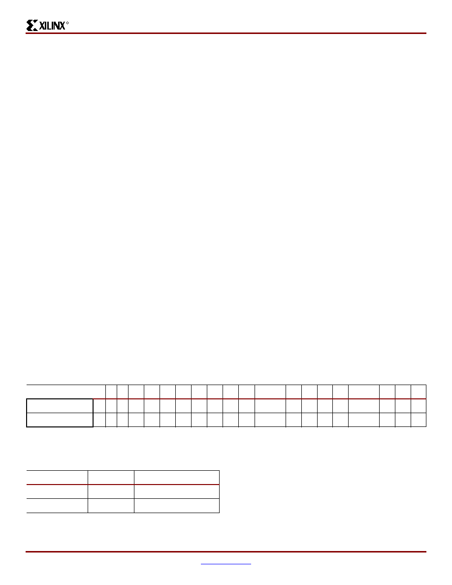
Table 3:
CLB/Block RAM Column Locations
Virtex-E Device
0
4
8
12
16
20
24
28
32
36
40
444852566064
68
72
76
80
84
XCV405E
√ √ √ √
√
√√√√√
XCV812E
√ √ √ √
√
√√√√√√√√√√
Table 4:
Virtex-E Block SelectRAM Amounts
Virtex-E Device
# of Blocks
Block SelectRAM Bits
XCV405E
140
573,440
XCV812E
280
1,146,880
相关PDF资料 |
PDF描述 |
|---|---|
| BR93L86RFVT-WE2 | IC EEPROM 16KBIT 2MHZ 8TSSOP |
| XCV405E-6FG676I | IC FPGA 1.8V 676-BGA |
| BR93L86RFVM-WTR | IC EEPROM 16KBIT 2MHZ 8MSOP |
| BR93L86RFV-WE2 | IC EEPROM 16KBIT 2MHZ 8SSOP |
| BR25L020FV-WE2 | IC EEPROM SER 2KB SPI BUS 8SSOP |
相关代理商/技术参数 |
参数描述 |
|---|---|
| XCV405E-7FG676I | 功能描述:IC FPGA 1.8V 676-BGA RoHS:否 类别:集成电路 (IC) >> 嵌入式 - FPGA(现场可编程门阵列) 系列:Virtex®-E EM 产品变化通告:Step Intro and Pkg Change 11/March/2008 标准包装:1 系列:Virtex®-5 SXT LAB/CLB数:4080 逻辑元件/单元数:52224 RAM 位总计:4866048 输入/输出数:480 门数:- 电源电压:0.95 V ~ 1.05 V 安装类型:表面贴装 工作温度:-40°C ~ 100°C 封装/外壳:1136-BBGA,FCBGA 供应商设备封装:1136-FCBGA 配用:568-5088-ND - BOARD DEMO DAC1408D750122-1796-ND - EVALUATION PLATFORM VIRTEX-5 |
| XCV405E-7FG900C | 制造商:XILINX 制造商全称:XILINX 功能描述:Virtex-E 1.8 V Extended Memory Field Programmable Gate Arrays |
| XCV405E-7FG900I | 制造商:XILINX 制造商全称:XILINX 功能描述:Virtex-E 1.8 V Extended Memory Field Programmable Gate Arrays |
| XCV405E-8BG404C | 制造商:XILINX 制造商全称:XILINX 功能描述:Virtex-E 1.8 V Extended Memory Field Programmable Gate Arrays |
| XCV405E-8BG404I | 制造商:XILINX 制造商全称:XILINX 功能描述:Virtex-E 1.8 V Extended Memory Field Programmable Gate Arrays |
发布紧急采购,3分钟左右您将得到回复。