参数资料
| 型号: | XCV405E-7FG676C |
| 厂商: | Xilinx Inc |
| 文件页数: | 17/118页 |
| 文件大小: | 0K |
| 描述: | IC FPGA 1.8V C-TEMP 676-FBGA |
| 产品变化通告: | FPGA Family Discontinuation 18/Apr/2011 |
| 标准包装: | 1 |
| 系列: | Virtex®-E EM |
| LAB/CLB数: | 2400 |
| 逻辑元件/单元数: | 10800 |
| RAM 位总计: | 573440 |
| 输入/输出数: | 404 |
| 门数: | 129600 |
| 电源电压: | 1.71 V ~ 1.89 V |
| 安装类型: | 表面贴装 |
| 工作温度: | 0°C ~ 85°C |
| 封装/外壳: | 676-BGA |
| 供应商设备封装: | 676-FBGA(27x27) |
第1页第2页第3页第4页第5页第6页第7页第8页第9页第10页第11页第12页第13页第14页第15页第16页当前第17页第18页第19页第20页第21页第22页第23页第24页第25页第26页第27页第28页第29页第30页第31页第32页第33页第34页第35页第36页第37页第38页第39页第40页第41页第42页第43页第44页第45页第46页第47页第48页第49页第50页第51页第52页第53页第54页第55页第56页第57页第58页第59页第60页第61页第62页第63页第64页第65页第66页第67页第68页第69页第70页第71页第72页第73页第74页第75页第76页第77页第78页第79页第80页第81页第82页第83页第84页第85页第86页第87页第88页第89页第90页第91页第92页第93页第94页第95页第96页第97页第98页第99页第100页第101页第102页第103页第104页第105页第106页第107页第108页第109页第110页第111页第112页第113页第114页第115页第116页第117页第118页
Virtex-E 1.8 V Extended Memory Field Programmable Gate Arrays
DS025-4 (v3.0) March 21, 2014
Module 4 of 4
37
R
— OBSOLETE — OBSOLETE — OBSOLETE — OBSOLETE —
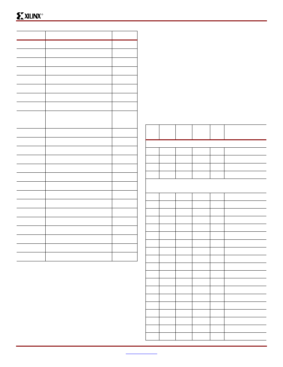
FG900 Differential Pin Pairs
Virtex-E Extended Memory devices have differential pin
pairs that can also provide other functions when not used as
a differential pair. A
√ in the AO column indicates that the pin
pair can be used as an asynchronous output for all devices
provided in this package.
Pairs with a note number in the AO column are device
dependent. They can have asynchronous outputs if the pin
pair is in the same CLB row and column in the device. Num-
bers in this column refer to footnotes that indicate which
devices have pin pairs that can be asynchronous outputs.
The Other Functions column indicates alternative func-
tion(s) not available when the pair is used as a differential
pair or differential clock.
NA
GND
AC8
NA
GND
H8
NA
GND
AD7
NA
GND
B8
NA
GND
AE6
NA
GND
G7
NA
GND
F6
NA
GND
AF5
NA
GND
E5
NA
GND
AG4
NA
GND
D4
NA
GND
V3
NA
GND
N3
NA
GND
C3
NA
GND
AK2
NA
GND
AH3
NA
GND
AC2
NA
GND
H2
NA
GND
B2
NA
GND
A2
NA
GND
AK1
NA
GND
AJ2
NA
GND
AJ1
NA
GND
A1
NA
GND
B1
Table 5:
FG900 Fine-Pitch BGA Package — XCV812E
Bank
Description
Pin
Table 6:
FG900 Differential Pin Pair Summary —
XCV812E
Pair
Bank
P
Pin
N
Pin
AO
Other
Functions
GCLK LVDS
3
0
C15
A15
NA
IO LVDS 34
2
1
E15
E16
NA
IO LVDS 34
1
5
AK16
AH16
NA
IO LVDS 177
0
4
AJ16
AF16
NA
IO LVDS 177
IO LVDS
Total Pairs: 235, Asynchronous Output Pairs: 85
10
G8
D5
√
-
20
H9
A3
√
-
40
D6
A4
√
-
50
B5
E7
√
VREF
60
F8
A5
-
70
N11
D7
-
80
E8
G9
√
-
90
J11
A6
√
VREF
10
0
B7
C7
-
11
0
H10
C8
-
12
0
F10
G10
√
-
13
0
H11
A8
√
VREF
15
0
J12
B9
-
17
0
B10
G11
-
19
0
F11
H13
√
-
20
0
D11
E11
√
-
22
0
C11
F12
√
-
23
0
D12
A10
√
VREF
24
0
A11
E12
-
相关PDF资料 |
PDF描述 |
|---|---|
| BR93L86RFVT-WE2 | IC EEPROM 16KBIT 2MHZ 8TSSOP |
| XCV405E-6FG676I | IC FPGA 1.8V 676-BGA |
| BR93L86RFVM-WTR | IC EEPROM 16KBIT 2MHZ 8MSOP |
| BR93L86RFV-WE2 | IC EEPROM 16KBIT 2MHZ 8SSOP |
| BR25L020FV-WE2 | IC EEPROM SER 2KB SPI BUS 8SSOP |
相关代理商/技术参数 |
参数描述 |
|---|---|
| XCV405E-7FG676I | 功能描述:IC FPGA 1.8V 676-BGA RoHS:否 类别:集成电路 (IC) >> 嵌入式 - FPGA(现场可编程门阵列) 系列:Virtex®-E EM 产品变化通告:Step Intro and Pkg Change 11/March/2008 标准包装:1 系列:Virtex®-5 SXT LAB/CLB数:4080 逻辑元件/单元数:52224 RAM 位总计:4866048 输入/输出数:480 门数:- 电源电压:0.95 V ~ 1.05 V 安装类型:表面贴装 工作温度:-40°C ~ 100°C 封装/外壳:1136-BBGA,FCBGA 供应商设备封装:1136-FCBGA 配用:568-5088-ND - BOARD DEMO DAC1408D750122-1796-ND - EVALUATION PLATFORM VIRTEX-5 |
| XCV405E-7FG900C | 制造商:XILINX 制造商全称:XILINX 功能描述:Virtex-E 1.8 V Extended Memory Field Programmable Gate Arrays |
| XCV405E-7FG900I | 制造商:XILINX 制造商全称:XILINX 功能描述:Virtex-E 1.8 V Extended Memory Field Programmable Gate Arrays |
| XCV405E-8BG404C | 制造商:XILINX 制造商全称:XILINX 功能描述:Virtex-E 1.8 V Extended Memory Field Programmable Gate Arrays |
| XCV405E-8BG404I | 制造商:XILINX 制造商全称:XILINX 功能描述:Virtex-E 1.8 V Extended Memory Field Programmable Gate Arrays |
发布紧急采购,3分钟左右您将得到回复。