参数资料
| 型号: | XCV405E-7FG676C |
| 厂商: | Xilinx Inc |
| 文件页数: | 46/118页 |
| 文件大小: | 0K |
| 描述: | IC FPGA 1.8V C-TEMP 676-FBGA |
| 产品变化通告: | FPGA Family Discontinuation 18/Apr/2011 |
| 标准包装: | 1 |
| 系列: | Virtex®-E EM |
| LAB/CLB数: | 2400 |
| 逻辑元件/单元数: | 10800 |
| RAM 位总计: | 573440 |
| 输入/输出数: | 404 |
| 门数: | 129600 |
| 电源电压: | 1.71 V ~ 1.89 V |
| 安装类型: | 表面贴装 |
| 工作温度: | 0°C ~ 85°C |
| 封装/外壳: | 676-BGA |
| 供应商设备封装: | 676-FBGA(27x27) |
第1页第2页第3页第4页第5页第6页第7页第8页第9页第10页第11页第12页第13页第14页第15页第16页第17页第18页第19页第20页第21页第22页第23页第24页第25页第26页第27页第28页第29页第30页第31页第32页第33页第34页第35页第36页第37页第38页第39页第40页第41页第42页第43页第44页第45页当前第46页第47页第48页第49页第50页第51页第52页第53页第54页第55页第56页第57页第58页第59页第60页第61页第62页第63页第64页第65页第66页第67页第68页第69页第70页第71页第72页第73页第74页第75页第76页第77页第78页第79页第80页第81页第82页第83页第84页第85页第86页第87页第88页第89页第90页第91页第92页第93页第94页第95页第96页第97页第98页第99页第100页第101页第102页第103页第104页第105页第106页第107页第108页第109页第110页第111页第112页第113页第114页第115页第116页第117页第118页
Virtex-E 1.8 V Extended Memory Field Programmable Gate Arrays
DS025-2 (v3.0) March 21, 2014
Module 2 of 4
29
R
— OBSOLETE — OBSOLETE — OBSOLETE — OBSOLETE —
Initialization
The block SelectRAM+ memory can initialize during the
device configuration sequence. The 16 initialization properties
of 64 hex values each (a total of 4096 bits) set the initialization
of each RAM. These properties appear in Table 17. Any initial-
ization properties not explicitly set configure as zeros. Partial
initialization strings pad with zeros. Initialization strings
greater than 64 hex values generate an error. The RAMs can
be simulated with the initialization values using generics in
VHDL simulators and parameters in Verilog simulators.
Initialization in VHDL and Synopsys
The block SelectRAM+ structures can be initialized in VHDL
for both simulation and synthesis for inclusion in the EDIF
output file. The simulation of the VHDL code uses a generic
to pass the initialization. Synopsys FPGA compiler does not
presently support generics. The initialization values instead
attach as attributes to the RAM by a built-in Synopsys
dc_script. The translate_off statement stops synthesis
translation of the generic statements. The following code
illustrates a module that employs these techniques.
Initialization in Verilog and Synopsys
The block SelectRAM+ structures can be initialized in Verilog
for both simulation and synthesis for inclusion in the EDIF
output file. The simulation of the Verilog code uses a def-
param to pass the initialization. The Synopsys FPGA com-
piler does not presently support defparam. The initialization
values instead attach as attributes to the RAM by a built-in
Synopsys dc_script. The translate_off statement stops syn-
thesis translation of the defparam statements. The following
code illustrates a module that employs these techniques.
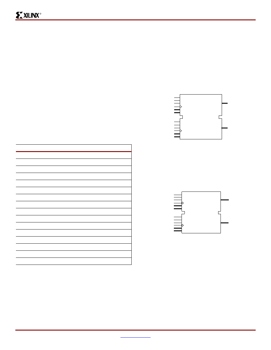
Design Examples
Creating a 32-bit Single-Port RAM
The true dual-read/write port functionality of the block
SelectRAM+ memory allows a single port, 128 deep by
32-bit wide RAM to be created using a single block
SelectRAM+ cell as shown inTable 35.
Interleaving the memory space, setting the LSB of the
address bus of Port A to 1 (VCC), and the LSB of the
address bus of Port B to 0 (GND), allows a 32-bit wide sin-
gle port RAM to be created.
Creating Two Single-Port RAMs
The true dual-read/write port functionality of the block
SelectRAM+ memory allows a single RAM to be split into two
single port memories of 2K bits each as shown in Figure 36.
In this example, a 512K x 4 RAM (Port A) and a 128 x 16
RAM (Port B) are created out of a single block SelectRAM+.
The address space for the RAM is split by fixing the MSB of
Port A to 1 (VCC) for the upper 2K bits and the MSB of Port
B to 0 (GND) for the lower 2K bits.
Block Memory Generation
The CoreGen program generates memory structures using
the block SelectRAM+ features. This program outputs
VHDL or Verilog simulation code templates and an EDIF file
for inclusion in a design.
Table 17:
RAM Initialization Properties
Property
Memory Cells
INIT_00
255 to 0
INIT_01
511 to 256
INIT_02
767 to 512
INIT_03
1023 to 768
INIT_04
1279 to 1024
INIT_05
1535 to 1280
INIT_06
1791 to 2047
INIT_07
2047 to 1792
INIT_08
2303 to 2048
INIT_09
2559 to 2304
INIT_0a
2815 to 2560
INIT_0b
3071 to 2816
INIT_0c
3327 to 3072
INIT_0d
3583 to 3328
INIT_0e
3839 to 3584
INIT_0f
4095 to 3840
Figure 35: Single Port 128 x 32 RAM
Figure 36: 512 x 4 RAM and 128 x 16 RAM
WEB
ENB
RSTB
CLKB
ADDRB[7:0]
DIB[15:0]
WEA
ENA
RSTA
CLKA
ADDRA[7:0]
DIA[15:0]
ADDR[6:0], V
CC
CLK
EN
RST
WE
CLK
EN
RST
WE
DI[31:16]
ADDR[6:0], GND
DI[15:0]
DOA[15:0]
DO[31:16]
DO[15:0]
DOB[15:0]
RAMB4_S16_S16
ds022_036_121399
WEB
ENB
RSTB
CLKB
ADDRB[7:0]
DIB[15:0]
WEA
ENA
RSTA
CLKA
ADDRA[9:0]
DIA[3:0]
V
CC, ADDR1[8:0]
DI1[3:0]
WE1
EN1
RST1
CLK1
WE2
EN2
RST2
CLK2
GND, ADDR2[6:0]
DI2[15:0]
DOA[3:0]
DO1[3:0]
DO2[15:0]
DOB[15:0]
RAMB4_S4_S16
ds022_037_121399
相关PDF资料 |
PDF描述 |
|---|---|
| BR93L86RFVT-WE2 | IC EEPROM 16KBIT 2MHZ 8TSSOP |
| XCV405E-6FG676I | IC FPGA 1.8V 676-BGA |
| BR93L86RFVM-WTR | IC EEPROM 16KBIT 2MHZ 8MSOP |
| BR93L86RFV-WE2 | IC EEPROM 16KBIT 2MHZ 8SSOP |
| BR25L020FV-WE2 | IC EEPROM SER 2KB SPI BUS 8SSOP |
相关代理商/技术参数 |
参数描述 |
|---|---|
| XCV405E-7FG676I | 功能描述:IC FPGA 1.8V 676-BGA RoHS:否 类别:集成电路 (IC) >> 嵌入式 - FPGA(现场可编程门阵列) 系列:Virtex®-E EM 产品变化通告:Step Intro and Pkg Change 11/March/2008 标准包装:1 系列:Virtex®-5 SXT LAB/CLB数:4080 逻辑元件/单元数:52224 RAM 位总计:4866048 输入/输出数:480 门数:- 电源电压:0.95 V ~ 1.05 V 安装类型:表面贴装 工作温度:-40°C ~ 100°C 封装/外壳:1136-BBGA,FCBGA 供应商设备封装:1136-FCBGA 配用:568-5088-ND - BOARD DEMO DAC1408D750122-1796-ND - EVALUATION PLATFORM VIRTEX-5 |
| XCV405E-7FG900C | 制造商:XILINX 制造商全称:XILINX 功能描述:Virtex-E 1.8 V Extended Memory Field Programmable Gate Arrays |
| XCV405E-7FG900I | 制造商:XILINX 制造商全称:XILINX 功能描述:Virtex-E 1.8 V Extended Memory Field Programmable Gate Arrays |
| XCV405E-8BG404C | 制造商:XILINX 制造商全称:XILINX 功能描述:Virtex-E 1.8 V Extended Memory Field Programmable Gate Arrays |
| XCV405E-8BG404I | 制造商:XILINX 制造商全称:XILINX 功能描述:Virtex-E 1.8 V Extended Memory Field Programmable Gate Arrays |
发布紧急采购,3分钟左右您将得到回复。