参数资料
| 型号: | XCV405E-7FG676C |
| 厂商: | Xilinx Inc |
| 文件页数: | 40/118页 |
| 文件大小: | 0K |
| 描述: | IC FPGA 1.8V C-TEMP 676-FBGA |
| 产品变化通告: | FPGA Family Discontinuation 18/Apr/2011 |
| 标准包装: | 1 |
| 系列: | Virtex®-E EM |
| LAB/CLB数: | 2400 |
| 逻辑元件/单元数: | 10800 |
| RAM 位总计: | 573440 |
| 输入/输出数: | 404 |
| 门数: | 129600 |
| 电源电压: | 1.71 V ~ 1.89 V |
| 安装类型: | 表面贴装 |
| 工作温度: | 0°C ~ 85°C |
| 封装/外壳: | 676-BGA |
| 供应商设备封装: | 676-FBGA(27x27) |
第1页第2页第3页第4页第5页第6页第7页第8页第9页第10页第11页第12页第13页第14页第15页第16页第17页第18页第19页第20页第21页第22页第23页第24页第25页第26页第27页第28页第29页第30页第31页第32页第33页第34页第35页第36页第37页第38页第39页当前第40页第41页第42页第43页第44页第45页第46页第47页第48页第49页第50页第51页第52页第53页第54页第55页第56页第57页第58页第59页第60页第61页第62页第63页第64页第65页第66页第67页第68页第69页第70页第71页第72页第73页第74页第75页第76页第77页第78页第79页第80页第81页第82页第83页第84页第85页第86页第87页第88页第89页第90页第91页第92页第93页第94页第95页第96页第97页第98页第99页第100页第101页第102页第103页第104页第105页第106页第107页第108页第109页第110页第111页第112页第113页第114页第115页第116页第117页第118页
Virtex-E 1.8 V Extended Memory Field Programmable Gate Arrays
Module 2 of 4
DS025-2 (v3.0) March 21, 2014
24
R
— OBSOLETE — OBSOLETE — OBSOLETE — OBSOLETE —
Board-level de-skew is not required for low-fanout clock net-
works. It is recommended for systems that have fanout lim-
itations on the clock network, or if the clock distribution chip
cannot handle the load.
Do not use the DLL output clock signals until after activation
of the LOCKED signal. Prior to the activation of the
LOCKED signal, the DLL output clocks are not valid and
can exhibit glitches, spikes, or other spurious movement.
The dll_mirror_1 files in the xapp132.zip file show the VHDL
and Verilog implementation of this circuit.
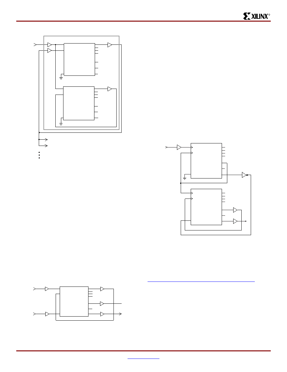
De-Skew of Clock and Its 2x Multiple
The circuit shown in Figure 29 implements a 2x clock multi-
plier and also uses the CLK0 clock output with zero ns skew
between registers on the same chip. A clock divider circuit
could alternatively be implemented using similar connec-
tions.
Because any single DLL can access only two BUFGs at
most, any additional output clock signals must be routed
from the DLL in this example on the high speed backbone
routing.
The dll_2x files in the xapp132.zip file show the VHDL and
Verilog implementation of this circuit.
Virtex-E 4x Clock
Two DLLs located in the same half-edge (top-left, top-right,
bottom-right, bottom-left) can be connected together, with-
out using a BUFG between the CLKDLLs, to generate a 4x
clock as shown in Figure 30. Virtex-E devices, like the Virtex
devices, have four clock networks that are available for inter-
nal de-skewing of the clock. Each of the eight DLLs have
access to two of the four clock networks. Although all the
DLLs can be used for internal de-skewing, the presence of
two GCLKBUFs on the top and two on the bottom indicate
that only two of the four DLLs on the top (and two of the four
DLLs on the bottom) can be used for this purpose.
The dll_4xe files in the xapp 32.zip file show the DLL imple-
mentation in Verilog for Virtex-E devices. These files can be
found at:
Using Block SelectRAM+ Features
The Virtex FPGA Series provides dedicated blocks of
on-chip, true dual-read/write port synchronous RAM, with
4096 memory cells. Each port of the block SelectRAM+
memory can be independently configured as a read/write
port, a read port, a write port, and can be configured to a
specific data width. block SelectRAM+ memory offers new
capabilities, allowing FPGA designers to simplify designs.
Figure 28: DLL De-skew of Board Level Clock
Figure 29: DLL De-skew of Clock and 2x Multiple
ds022_029_121099
CLK0
CLK90
CLK180
CLK270
CLK2X
CLKDV
LOCKED
CLKIN
CLKFB
RST
CLKDLL
OBUF
IBUFG
CLK0
CLK90
CLK180
CLK270
CLK2X
CLKDV
LOCKED
CLKIN
CLKFB
RST
CLKDLL
BUFG
IBUFG
Non-Virtex-E Chip
Other Non_Virtex-E Chips
Virtex-E Device
CLK0
CLK90
CLK180
CLK270
CLK2X
CLKDV
LOCKED
CLKIN
CLKFB
RST
ds022_030_121099
CLKDLL
BUFG
IBUFG
IBUF
OBUF
BUFG
Figure 30: DLL Generation of 4x Clock in Virtex-E
Devices
ds022_031_041901
RST
CLKFB
CLKIN
CLKDLL-S
LOCKED
CLKDV
INV
BUFG
OBUF
IBUFG
CLK2X
CLK0
CLK90
CLK180
CLK270
RST
CLKFB
CLKIN
CLKDLL-P
LOCKED
CLKDV
CLK2X
CLK0
CLK90
CLK180
CLK270
相关PDF资料 |
PDF描述 |
|---|---|
| BR93L86RFVT-WE2 | IC EEPROM 16KBIT 2MHZ 8TSSOP |
| XCV405E-6FG676I | IC FPGA 1.8V 676-BGA |
| BR93L86RFVM-WTR | IC EEPROM 16KBIT 2MHZ 8MSOP |
| BR93L86RFV-WE2 | IC EEPROM 16KBIT 2MHZ 8SSOP |
| BR25L020FV-WE2 | IC EEPROM SER 2KB SPI BUS 8SSOP |
相关代理商/技术参数 |
参数描述 |
|---|---|
| XCV405E-7FG676I | 功能描述:IC FPGA 1.8V 676-BGA RoHS:否 类别:集成电路 (IC) >> 嵌入式 - FPGA(现场可编程门阵列) 系列:Virtex®-E EM 产品变化通告:Step Intro and Pkg Change 11/March/2008 标准包装:1 系列:Virtex®-5 SXT LAB/CLB数:4080 逻辑元件/单元数:52224 RAM 位总计:4866048 输入/输出数:480 门数:- 电源电压:0.95 V ~ 1.05 V 安装类型:表面贴装 工作温度:-40°C ~ 100°C 封装/外壳:1136-BBGA,FCBGA 供应商设备封装:1136-FCBGA 配用:568-5088-ND - BOARD DEMO DAC1408D750122-1796-ND - EVALUATION PLATFORM VIRTEX-5 |
| XCV405E-7FG900C | 制造商:XILINX 制造商全称:XILINX 功能描述:Virtex-E 1.8 V Extended Memory Field Programmable Gate Arrays |
| XCV405E-7FG900I | 制造商:XILINX 制造商全称:XILINX 功能描述:Virtex-E 1.8 V Extended Memory Field Programmable Gate Arrays |
| XCV405E-8BG404C | 制造商:XILINX 制造商全称:XILINX 功能描述:Virtex-E 1.8 V Extended Memory Field Programmable Gate Arrays |
| XCV405E-8BG404I | 制造商:XILINX 制造商全称:XILINX 功能描述:Virtex-E 1.8 V Extended Memory Field Programmable Gate Arrays |
发布紧急采购,3分钟左右您将得到回复。