- 您现在的位置:买卖IC网 > PDF目录16433 > XR16V798IQ-0B-EVB (Exar Corporation)EVAL BOARD FOR XR16V798-B 100QFP PDF资料下载
参数资料
| 型号: | XR16V798IQ-0B-EVB |
| 厂商: | Exar Corporation |
| 文件页数: | 16/56页 |
| 文件大小: | 0K |
| 描述: | EVAL BOARD FOR XR16V798-B 100QFP |
| 设计资源: | XR17V798/794 Eval Board Schematic |
| 标准包装: | 1 |
| 系列: | * |
第1页第2页第3页第4页第5页第6页第7页第8页第9页第10页第11页第12页第13页第14页第15页当前第16页第17页第18页第19页第20页第21页第22页第23页第24页第25页第26页第27页第28页第29页第30页第31页第32页第33页第34页第35页第36页第37页第38页第39页第40页第41页第42页第43页第44页第45页第46页第47页第48页第49页第50页第51页第52页第53页第54页第55页第56页
XR16V798
23
REV. 1.0.1
HIGH PERFORMANCE 2.25V TO 3.6V OCTAL UART WITH FRACTIONAL BAUD RATE
3.1.1.1
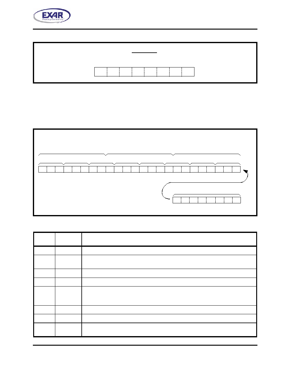
INT0 Channel Interrupt Indicator:
3.1.1.2
INT1, INT2 and INT3 Interrupt Source Locator
INT3, INT2 and INT1 provide a 24-bit (3 bits per channel) encoded interrupt indicator. Table 9 shows the 3 bit
encoding and their priority order. The 16-bit Timer time-out interrupt will show up only as a channel 0 interrupt.
For other channels, interrupt 7 is reserved.
.
FIGURE 13. THE GLOBAL INTERRUPT REGISTERS, INT0, INT1, INT2 AND INT3
TABLE 9: UART CHANNEL [7:0] INTERRUPT SOURCE ENCODING AND CLEARING
PRIORITY
Bit
2
Bit
1
Bit
0
INTERRUPT SOURCE(S) AND CLEARING
x
0
None or wake-up indicator
1
0
1
RXRDY & RX Line Status (logic OR of LSR[4:1]). RXRDY INT clears by reading data in the RX
FIFO until it falls below the trigger level; RX Line Status INT cleared after reading LSR register.
2
0
1
0
RXRDY Time-out: Cleared same way as RXRDY INT.
3
0
1
TXRDY, THR or TSR (auto RS485 mode) empty, clears after reading ISR register.
4
1
0
MSR, RTS/CTS or DTR/DSR delta or Xoff/Xon or special character detected. The first two
clears after reading MSR register; Xoff/Xon or special char. detect INT clears after reading ISR
register.
5
1
0
1
Reserved.
6
1
0
Reserved.
7
1
TIMER Time-out, shows up as a channel 0 INT. It clears after reading the TIMERCNTL register.
Reserved in other channels.
INT0 Register
Individual UART Channel Interrupt Status
Ch-7
Ch-6
Ch-5
Ch-4
Ch-3
Ch-2
Ch-1
Ch-0
Bit-7
Bit-6
Bit-5
Bit-4
Bit-3
Bit-2
Bit-1
Bit-0
Channel-7
Channel-6
Channel-5
Channel-4
Channel-3
Channel-2
Channel-1
Channel-0
INT2 Register
INT1 Register
INT3 Register
Interrupt Registers,
INT0, INT1, INT2 and INT3
Bit
1
Bit
2
Bit
0
Bit
1
Bit
2
Bit
0
Bit
1
Bit
2
Bit
0
Bit
1
Bit
2
Bit
0
Bit
1
Bit
2
Bit
0
Bit
1
Bit
2
Bit
0
Bit
1
Bit
2
Bit
0
Bit
1
Bit
2
Bit
0
INT0 Register
Bit-0
Bit-1
Bit-2
Bit-3
Bit-7
Bit-4
Bit-5
Bit-6
Ch-6
Ch-7
Ch-5 Ch-4
Ch-1 Ch-0
Ch-3 Ch-2
相关PDF资料 |
PDF描述 |
|---|---|
| XR16V798IQ-0A-EVB | EVAL BOARD FOR XR16V798-A 100QFP |
| XR16V698IQ-0B-EVB | EVAL BOARD FOR XR16V698-B 100QFP |
| XR16V698IQ-0A-EVB | EVAL BOARD FOR XR16V698-A 100QFP |
| KIT33972AEWEVBE | KIT EVALUATION FOR MC33972 |
| EBM31DCMS | CONN EDGECARD 62POS .156 WW |
相关代理商/技术参数 |
参数描述 |
|---|---|
| XR16V798IQ-F | 功能描述:UART 接口集成电路 UART RoHS:否 制造商:Texas Instruments 通道数量:2 数据速率:3 Mbps 电源电压-最大:3.6 V 电源电压-最小:2.7 V 电源电流:20 mA 最大工作温度:+ 85 C 最小工作温度:- 40 C 封装 / 箱体:LQFP-48 封装:Reel |
| XR16V798IQTR-F | 制造商:Exar Corporation 功能描述:UART 8-CH 64Byte FIFO 2.5V/3.3V 100-Pin PQFP T/R |
| XR-1790 | 制造商:未知厂家 制造商全称:未知厂家 功能描述:Audio Schematic |
| XR17C152 | 制造商:EXAR 制造商全称:EXAR 功能描述:5V PCI BUS DUAL UART |
| XR17C152CM | 制造商:EXAR 制造商全称:EXAR 功能描述:5V PCI BUS DUAL UART |
发布紧急采购,3分钟左右您将得到回复。