参数资料
| 型号: | XRD98L61AIV-F |
| 厂商: | Exar Corporation |
| 文件页数: | 11/38页 |
| 文件大小: | 0K |
| 描述: | IC CCD DIGITIZER 12BIT 48TQFP |
| 标准包装: | 250 |
| 位数: | 12 |
| 通道数: | 1 |
| 电压 - 电源,模拟: | 2.7 V ~ 3.6 V |
| 电压 - 电源,数字: | 2.7 V ~ 3.6 V |
| 封装/外壳: | 48-TQFP |
| 供应商设备封装: | 48-TQFP(7x7) |
| 包装: | 托盘 |
第1页第2页第3页第4页第5页第6页第7页第8页第9页第10页当前第11页第12页第13页第14页第15页第16页第17页第18页第19页第20页第21页第22页第23页第24页第25页第26页第27页第28页第29页第30页第31页第32页第33页第34页第35页第36页第37页第38页
19
Rev. 2.00
XRD98L61
DIRECT PGA INPUT MODE
The inputs to the PGA can be accessed directly
(bypassing the CDS) through the Test1 & Test2 pins
(See Figure 1). The test inputs require Test2 set to a
dc voltage of 1.2V and the Test1 input signal between
1.2V and 0.4V. ADC Zero Scale (000h) is at 1.2V input
and Full Scale (FFFh)for a 0.4V input assuming a gain
of 8dB. (ADC full scale input is 2Vpp.)
To enable the Direct PGA Input mode, write a “1” to the
NoCDS bit in the Control register of the serial interface.
This will disconnect the CDS from the PGA input and
turn on the switches that connect the Test1 & Test2
pins to the PGA. Note that when the part is not in the
NoCDS mode that Test1 and Test2 are grounded
through an equivalent 10kohm switch resistance. To
avoid shorting the input drive circuitry into Test1 and
Test2 to ground, the NoCDS mode must be active
before the input signal is driven.
In this mode, the SBLK and SPIX clocks must be
clocked, due to the switched capacitor architecture of
the second PGA stage. ADCLK must be provided to
digitize the PGA output. The analog PGA output
cannot be monitored; it does not come out to any pin.
The calibration logic should be put into the Hold mode,
or into the ManCAL mode. The Coarse offset correction
DAC (CDAC) is disconnected from the PGA inputs in
this mode. The CDAC does not affect the Direct PGA
inputs, but the Fine offset correction DAC (FDAC) does
affect the PGA output. The FDAC range is +-128mV
at the ADC input. FDAC can be used to adjust offset
in the system when in the ManCal mode.
Note the calibration logic should not be in the automatic
mode, because the FDAC circuitry is not “aware” that
the Coarse DAC is not active, and thus could cause
errors if left operating automatically. Therefore, it is
recommended that either CAL Hold or Manual CAL
mode be asserted.
The DNL in the Direct PGA Input Mode is shown in
Figure 26.
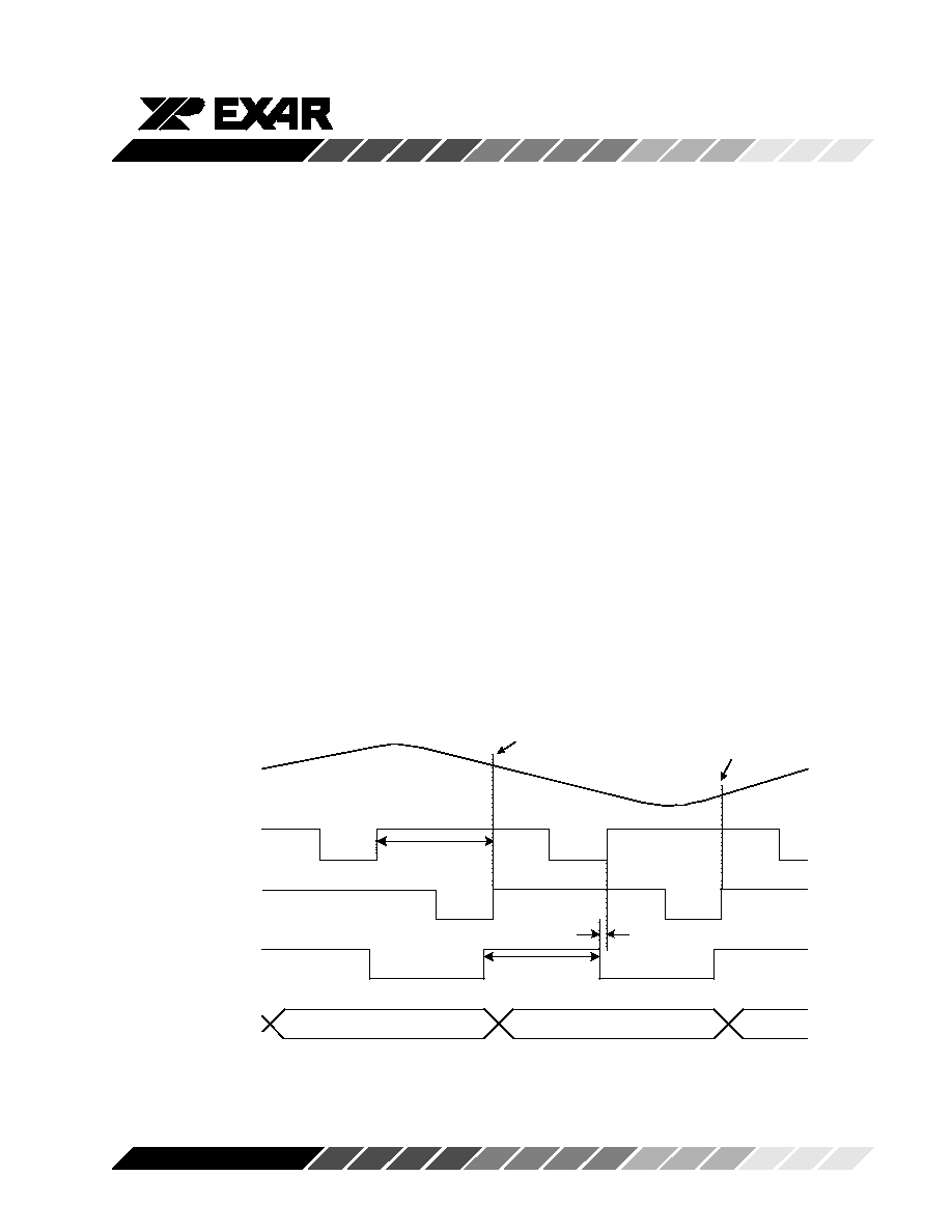
Figure 8. Direct PGA Input Timing (Default Polarities)
Input Signal
Test1
PGA tracks
Input Signal
Input Sampled (N)
Input Sampled
(N+1)
ADC tracks
PGA output
SPIX
ADCLK
SBLK
DB[11:0]
nonoverlap=4ns
(N-8)
(N-7)
(N-6)
相关PDF资料 |
PDF描述 |
|---|---|
| XRD98L62ACV-F | IC CCD DIGITIZER 12BIT 48TQFP |
| XRD98L63AIV-F | IC CCD DIGITIZER 12BIT 48TQFP |
| XRT71D00IQ-F | IC JITTER ATTENUATOR SGL 32TQFP |
| XRT71D03IV-F | IC JITTER ATTENUATOR 3CH 64TQFP |
| XRT71D04IV | IC JITTER ATTENUATOR 4CH 80TQFP |
相关代理商/技术参数 |
参数描述 |
|---|---|
| XRD98L61EVAL | 功能描述:数据转换 IC 开发工具 Eval Board for XRD98L61AIV RoHS:否 制造商:Texas Instruments 产品:Demonstration Kits 类型:ADC 工具用于评估:ADS130E08 接口类型:SPI 工作电源电压:- 6 V to + 6 V |
| XRD98L61ZEVAL | 功能描述:数据转换 IC 开发工具 Eval Board (Solder) XRD98L61AIV RoHS:否 制造商:Texas Instruments 产品:Demonstration Kits 类型:ADC 工具用于评估:ADS130E08 接口类型:SPI 工作电源电压:- 6 V to + 6 V |
| XRD98L62 | 制造商:EXAR 制造商全称:EXAR 功能描述:CCD Image Digitizers with CDS, PGA and 12-Bit A/D |
| XRD98L62ACV | 制造商:EXAR 制造商全称:EXAR 功能描述:CCD Image Digitizers with CDS, PGA and 12-Bit A/D |
| XRD98L62ACV-F | 功能描述:视频 IC RoHS:否 制造商:Fairchild Semiconductor 工作电源电压:5 V 电源电流:80 mA 最大工作温度:+ 85 C 封装 / 箱体:TSSOP-28 封装:Reel |
发布紧急采购,3分钟左右您将得到回复。