参数资料
| 型号: | XRD98L61AIV-F |
| 厂商: | Exar Corporation |
| 文件页数: | 21/38页 |
| 文件大小: | 0K |
| 描述: | IC CCD DIGITIZER 12BIT 48TQFP |
| 标准包装: | 250 |
| 位数: | 12 |
| 通道数: | 1 |
| 电压 - 电源,模拟: | 2.7 V ~ 3.6 V |
| 电压 - 电源,数字: | 2.7 V ~ 3.6 V |
| 封装/外壳: | 48-TQFP |
| 供应商设备封装: | 48-TQFP(7x7) |
| 包装: | 托盘 |
第1页第2页第3页第4页第5页第6页第7页第8页第9页第10页第11页第12页第13页第14页第15页第16页第17页第18页第19页第20页当前第21页第22页第23页第24页第25页第26页第27页第28页第29页第30页第31页第32页第33页第34页第35页第36页第37页第38页
XRD98L61
28
Rev. 2.00
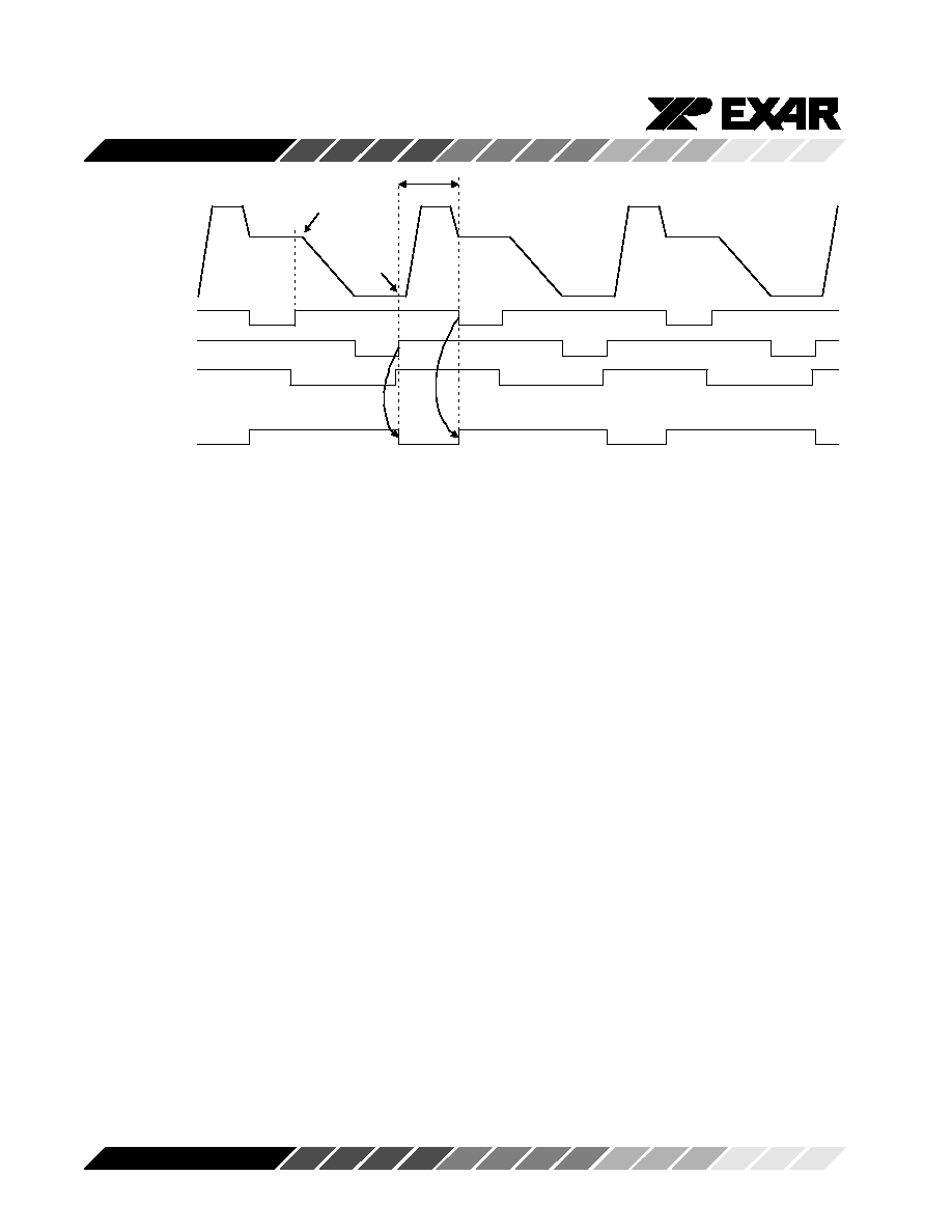
Figure 17. Pixel Rate Clock Timing with RSTreject=1
Reset Reject
In the default state, the reset reject switches (
φ3) are
always ON, they are not clocked. The reset pulse of
each pixel is transmitted to the first stage of the PGA.
Depending on the PGA gain and the actual voltage
level of the reset pulse, this could cause the first stage
of the PGA to rail. During the Black Level sampling, the
PGA should have enough time to recuperate, but as a
precaution, we have included the Reset Reject option.
When RSTreject = 1, the reset reject switches are
turned OFF at the end of the SPIX pulse, and turned ON
again at the start of the SBLK pulse. This will effec-
tively reject the reset pulse and prevent it from railing
the PGA.
Aperture Delays
One of the most difficult tasks in designing a digital
camera is optimizing the pixel timing for the CCD, CDS
and ADC. We have included the programmable aper-
ture delay function to help simplify this job.
There are two serial interface registers, DelayA &
DelayB, used to program the aperture delays. Each
register is divided into 3 delay parameters. Each delay
parameter is 3 bits wide. Each delay parameter can be
set to add from 0ns to 7ns of delay.
The delays are added to the clock signals after the
polarity control. This means the definition of leading
edge and trailing edge depends on the polarity control
bit for each clock. For the default case, SBLKpol=0 &
CCD Signal
SBLK
SPIX
ADCLK
Black Level
Video
Level
φ3
Reset Reject
Switches Turn OFF
SPIXpol=0, the leading edge is the falling edge and the
trailing edge is the rising edge.
DelayA[2:0] controls the delay added to the leading
edge of SBLK.
This positions the falling edge of
internal signal
φ1.
DelayA[5:3] controls the delay added to the trailing
edge of SBLK. This positions the rising edge of internal
signal
φ1.
DelayB[2:0] controls the delay added to the leading
edge of
φ2. This positions the falling edge of internal
signal
φ2.
DelayB[5:3] controls the delay added to the trailing
edge of SPIX. This positions the rising edge of internal
signal
φ2.
DelayB[8:6] is only used when SPIXopt=0. It controls
the delay from the trailing edge of SBLK to the start of
the internal
φ2 control. This delay is in addition to
DelayA[5:3], the SBLK trailing edge delay.
DelayA[8:6] controls the delay added to ADCLK. This
is a simple delay. It adds the same delay to both the
rising and falling edges of ADCLK to create
φ4.
相关PDF资料 |
PDF描述 |
|---|---|
| XRD98L62ACV-F | IC CCD DIGITIZER 12BIT 48TQFP |
| XRD98L63AIV-F | IC CCD DIGITIZER 12BIT 48TQFP |
| XRT71D00IQ-F | IC JITTER ATTENUATOR SGL 32TQFP |
| XRT71D03IV-F | IC JITTER ATTENUATOR 3CH 64TQFP |
| XRT71D04IV | IC JITTER ATTENUATOR 4CH 80TQFP |
相关代理商/技术参数 |
参数描述 |
|---|---|
| XRD98L61EVAL | 功能描述:数据转换 IC 开发工具 Eval Board for XRD98L61AIV RoHS:否 制造商:Texas Instruments 产品:Demonstration Kits 类型:ADC 工具用于评估:ADS130E08 接口类型:SPI 工作电源电压:- 6 V to + 6 V |
| XRD98L61ZEVAL | 功能描述:数据转换 IC 开发工具 Eval Board (Solder) XRD98L61AIV RoHS:否 制造商:Texas Instruments 产品:Demonstration Kits 类型:ADC 工具用于评估:ADS130E08 接口类型:SPI 工作电源电压:- 6 V to + 6 V |
| XRD98L62 | 制造商:EXAR 制造商全称:EXAR 功能描述:CCD Image Digitizers with CDS, PGA and 12-Bit A/D |
| XRD98L62ACV | 制造商:EXAR 制造商全称:EXAR 功能描述:CCD Image Digitizers with CDS, PGA and 12-Bit A/D |
| XRD98L62ACV-F | 功能描述:视频 IC RoHS:否 制造商:Fairchild Semiconductor 工作电源电压:5 V 电源电流:80 mA 最大工作温度:+ 85 C 封装 / 箱体:TSSOP-28 封装:Reel |
发布紧急采购,3分钟左右您将得到回复。