参数资料
| 型号: | XRD98L61AIV-F |
| 厂商: | Exar Corporation |
| 文件页数: | 9/38页 |
| 文件大小: | 0K |
| 描述: | IC CCD DIGITIZER 12BIT 48TQFP |
| 标准包装: | 250 |
| 位数: | 12 |
| 通道数: | 1 |
| 电压 - 电源,模拟: | 2.7 V ~ 3.6 V |
| 电压 - 电源,数字: | 2.7 V ~ 3.6 V |
| 封装/外壳: | 48-TQFP |
| 供应商设备封装: | 48-TQFP(7x7) |
| 包装: | 托盘 |
第1页第2页第3页第4页第5页第6页第7页第8页当前第9页第10页第11页第12页第13页第14页第15页第16页第17页第18页第19页第20页第21页第22页第23页第24页第25页第26页第27页第28页第29页第30页第31页第32页第33页第34页第35页第36页第37页第38页
17
Rev. 2.00
XRD98L61
φ1
φ2
CLAMP
Vbias1=1.2V
Vbias2
REFin
CCDin
PGA1
PGA2
CCD
Coarse
Offset
DAC
PGA
CDS
External
DC Blocking
Capacitors
Internal
Black Sample
Capacitors
φ3
Internal
Video Sample
Capacitors
φ2
DC Restore Switches
C1
C2
Fine
Offset
DAC
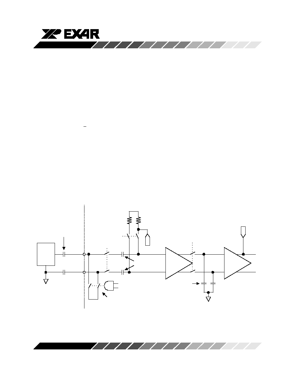
Figure 6. CDS and PGA Block Diagram
CORRELATED DOUBLE SAMPLE/HOLD (CDS)
The function of the CDS block is to sense the voltage
difference between the black level and video level for
each pixel. The PGA then amplifies this difference to
the desired level for the ADC. The CDS and PGA are
fully differential. The CCDin pin should be connected,
via a capacitor, to the CCD output signal. The REFin
pin should be connected, via a capacitor, to the CCD
“Common” voltage (typically the CCD ground is used
as the “Common” voltage). These capacitors, C1 and
C2, are typically 0.01
F + 10% or better matching.
The timing for the switches shown in Figure 6 are
determined by
φ1, φ2, and φ3. φ1, φ2, and φ3 are
internally generated from the timing signals SBLK and
SPIX shown in Figures 17 & 18.
φ3 (reset reject
switches) are closed to simplify the operation de-
scribed below.
At the beginning (or end) of every video line, the DC
restore switch forces one side of the external capaci-
tors to an internal bias level (Vbias1=1.2V). The DC
restore switch is controlled by the combination of the
CLAMP input signal ANDed with the
φ2 clock.
During the black reference phase of each CCD pixel,
the
φ1 (Sample Black Reference) switches are turned
on, shorting the PGA1 inputs to a second bias level
(Vbias2). The Coarse Offset DAC adds an adjustment
to the bias level (Vbias2) to cancel black level offset in
the CCD signal. When the
φ1 switches turn off, the
pixel black reference level is sampled on the internal
black sample capacitors, and the PGA is ready to gain
up the CCD video signal.
During the video phase of each CCD pixel, the differ-
ence between the pixel black level and video level is
transmitted through the internal black sample capaci-
tors and converted to a fully differential signal by the
PGA1 amplifier. At this time, the
φ2 (Sample Pixel
value) switches turn on, and the internal video sample
capacitors track the amplified difference. The Fine
Offset DAC adds offset adjustment to the PGA2 output
(post gain).
相关PDF资料 |
PDF描述 |
|---|---|
| XRD98L62ACV-F | IC CCD DIGITIZER 12BIT 48TQFP |
| XRD98L63AIV-F | IC CCD DIGITIZER 12BIT 48TQFP |
| XRT71D00IQ-F | IC JITTER ATTENUATOR SGL 32TQFP |
| XRT71D03IV-F | IC JITTER ATTENUATOR 3CH 64TQFP |
| XRT71D04IV | IC JITTER ATTENUATOR 4CH 80TQFP |
相关代理商/技术参数 |
参数描述 |
|---|---|
| XRD98L61EVAL | 功能描述:数据转换 IC 开发工具 Eval Board for XRD98L61AIV RoHS:否 制造商:Texas Instruments 产品:Demonstration Kits 类型:ADC 工具用于评估:ADS130E08 接口类型:SPI 工作电源电压:- 6 V to + 6 V |
| XRD98L61ZEVAL | 功能描述:数据转换 IC 开发工具 Eval Board (Solder) XRD98L61AIV RoHS:否 制造商:Texas Instruments 产品:Demonstration Kits 类型:ADC 工具用于评估:ADS130E08 接口类型:SPI 工作电源电压:- 6 V to + 6 V |
| XRD98L62 | 制造商:EXAR 制造商全称:EXAR 功能描述:CCD Image Digitizers with CDS, PGA and 12-Bit A/D |
| XRD98L62ACV | 制造商:EXAR 制造商全称:EXAR 功能描述:CCD Image Digitizers with CDS, PGA and 12-Bit A/D |
| XRD98L62ACV-F | 功能描述:视频 IC RoHS:否 制造商:Fairchild Semiconductor 工作电源电压:5 V 电源电流:80 mA 最大工作温度:+ 85 C 封装 / 箱体:TSSOP-28 封装:Reel |
发布紧急采购,3分钟左右您将得到回复。