- 您现在的位置:买卖IC网 > PDF目录293971 > 5962-9205805QXA (TEXAS INSTRUMENTS INC) 32-BIT, 60 MHz, OTHER DSP, CPGA141 PDF资料下载
参数资料
| 型号: | 5962-9205805QXA |
| 厂商: | TEXAS INSTRUMENTS INC |
| 元件分类: | 数字信号处理 |
| 英文描述: | 32-BIT, 60 MHz, OTHER DSP, CPGA141 |
| 封装: | STAGGERED, CERAMIC, PGA-141 |
| 文件页数: | 33/54页 |
| 文件大小: | 1033K |
| 代理商: | 5962-9205805QXA |
第1页第2页第3页第4页第5页第6页第7页第8页第9页第10页第11页第12页第13页第14页第15页第16页第17页第18页第19页第20页第21页第22页第23页第24页第25页第26页第27页第28页第29页第30页第31页第32页当前第33页第34页第35页第36页第37页第38页第39页第40页第41页第42页第43页第44页第45页第46页第47页第48页第49页第50页第51页第52页第53页第54页
SMJ320C31, SMJ320LC31, SMQ320LC31
DIGITAL SIGNAL PROCESSORS
SGUS026G APRIL 1998 REVISED SEPTEMBER 2006
39
POST OFFICE BOX 1443
HOUSTON, TEXAS 772511443
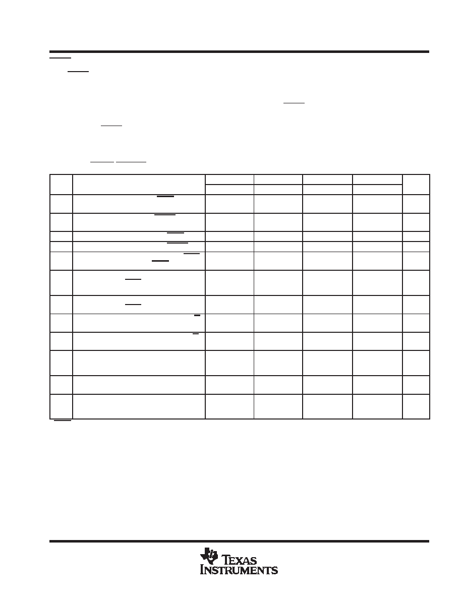
HOLD timing
HOLD is an asynchronous input that can be asserted at any time during a clock cycle. If the specified timings
are met, the exact sequence shown in Figure 27 occurs; otherwise, an additional delay of one clock cycle is
possible.
The NOHOLD bit of the primary-bus control register overrides the HOLD signal. When this bit is set, the device
comes out of hold and prevents future hold cycles.
Asserting HOLD prevents the processor from accessing the primary bus. Program execution continues until a
read from or a write to the primary bus is requested. In certain circumstances, the first write is pending, thus
allowing the processor to continue until a second write is encountered.
timing for HOLD/HOLDA (see Figure 28)
NO.
’C31-40
’LC31-40
’C31-50
’C31-60
UNIT
NO.
MIN
MAX
MIN
MAX
MIN
MAX
MIN
MAX
UNIT
69
tsu(HOLD-H1L)
Setup time, HOLD before
H1 low
13
10
8
ns
70
tv(H1L-HOLDA)
Valid time, HOLDA after H1
low
0
9
0*
9
0*
7
0*
6
ns
71
tw(HOLD)
Pulse duration, HOLD low
2tc(H)
ns
72
tw(HOLDA)
Pulse duration, HOLDA low
tcH5*
ns
73
td(H1L-SH)H
Delay time, H1 low to STRB
high for a HOLD
0*
9
0*
9
0*
7
0*
6
ns
74
tdis(H1L-S)
Disable time, H1 low to
STRB to the
high-impedance state
0*
9*
0*
9*
0*
7*
0*
7*
ns
75
ten(H1L-S)
Enable time, H1 low to
STRB enabled (active)
0*
9
0*
9
0*
7
0*
6
ns
76
tdis(H1L-RW)
Disable time, H1 low to R/W
to the high-impedance state
0*
9*
0*
9*
0*
8*
0*
7*
ns
77
ten(H1L-RW)
Enable time, H1 low to R/W
enabled (active)
0*
9
0*
9
0*
7
0*
6
ns
78
tdis(H1L-A)
Disable time, H1 low to
address to the
high-impedance state
0*
9*
0*
10*
0*
8*
0*
7*
ns
79
ten(H1L-A)
Enable time, H1 low to
address enabled (valid)
0*
13
0*
13
0*
10
0*
11?
ns
80
tdis(H1H-D)
Disable time, H1 high to
data to the high-impedance
state
0*
12*
0*
9*
0*
10*
0*
7*
ns
HOLD is an asynchronous input and can be asserted at any point during a clock cycle. If the specified timings are met, the exact sequence shown
in Figure 28 occurs; otherwise, an additional delay of one clock cycle is possible.
* This parameter is not production tested.
相关PDF资料 |
PDF描述 |
|---|---|
| 5962-9309101HYA | EEPROM 5V MODULE, CDIP32 |
| 5962-9315302MXX | 4K X 9 MULTI-PORT SRAM, 25 ns, CQCC |
| 596287663012X | ACT SERIES, 8-BIT TRANSCEIVER, TRUE OUTPUT, CQCC20 |
| 5962D0053605QYX | 512K X 8 STANDARD SRAM, 20 ns, CDFP36 |
| 5962D1022901QXC | 64M X 40 SYNCHRONOUS DRAM, 5.4 ns, CQFP128 |
相关代理商/技术参数 |
参数描述 |
|---|---|
| 5962-9205805QYA | 制造商:Texas Instruments 功能描述:DSP FLOATING PT 32BIT 60MHZ 30MIPS 132CFPAK - Rail/Tube |
| 596292062012MYC | 制造商:ALTERA 功能描述:EPM5192GM883B |
| 5962-92062012MYC | 制造商:ALTERA 功能描述:EPM5192GM883B |
| 5962-9206201MYC | 制造商:Cypress Semiconductor 功能描述:CPLD 192 Macro Cells 0.8um (CMOS) Technology 5V 84-Pin Windowed PGA |
| 5962-9206202MYC | 制造商:e2v Aerospace & Defense 功能描述:CPLD, UV ERASABLE, 192-MACROCELL, 30 NS PROP. DELAY TIME |
发布紧急采购,3分钟左右您将得到回复。