- 您现在的位置:买卖IC网 > PDF目录1887 > 73S1210F-68IMR/F/P (Maxim Integrated Products)IC SMART CARD READER PROG 68-QFN PDF资料下载
参数资料
| 型号: | 73S1210F-68IMR/F/P |
| 厂商: | Maxim Integrated Products |
| 文件页数: | 32/126页 |
| 文件大小: | 0K |
| 描述: | IC SMART CARD READER PROG 68-QFN |
| 产品培训模块: | Lead (SnPb) Finish for COTS Obsolescence Mitigation Program |
| 标准包装: | 2,500 |
| 系列: | 73S12xx |
| 核心处理器: | 80515 |
| 芯体尺寸: | 8-位 |
| 速度: | 24MHz |
| 连通性: | I²C,智能卡,UART/USART |
| 外围设备: | LED,POR,WDT |
| 输入/输出数: | 8 |
| 程序存储器容量: | 32KB(32K x 8) |
| 程序存储器类型: | 闪存 |
| RAM 容量: | 2K x 8 |
| 电压 - 电源 (Vcc/Vdd): | 2.7 V ~ 6.5 V |
| 振荡器型: | 内部 |
| 工作温度: | -40°C ~ 85°C |
| 封装/外壳: | 68-VFQFN 裸露焊盘 |
| 包装: | 带卷 (TR) |
第1页第2页第3页第4页第5页第6页第7页第8页第9页第10页第11页第12页第13页第14页第15页第16页第17页第18页第19页第20页第21页第22页第23页第24页第25页第26页第27页第28页第29页第30页第31页当前第32页第33页第34页第35页第36页第37页第38页第39页第40页第41页第42页第43页第44页第45页第46页第47页第48页第49页第50页第51页第52页第53页第54页第55页第56页第57页第58页第59页第60页第61页第62页第63页第64页第65页第66页第67页第68页第69页第70页第71页第72页第73页第74页第75页第76页第77页第78页第79页第80页第81页第82页第83页第84页第85页第86页第87页第88页第89页第90页第91页第92页第93页第94页第95页第96页第97页第98页第99页第100页第101页第102页第103页第104页第105页第106页第107页第108页第109页第110页第111页第112页第113页第114页第115页第116页第117页第118页第119页第120页第121页第122页第123页第124页第125页第126页
DS_1210F_001
73S1210F Data Sheet
Rev. 1.4
13
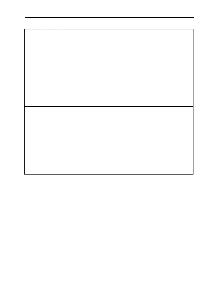
Table 3: Flash Special Function Registers
Register
SFR
Address
R/W
Description
ERASE
0x94
W
This register is used to initiate either the Flash Mass Erase cycle or the
Flash Page Erase cycle. Specific patterns are expected for ERASE in
order to initiate the appropriate Erase cycle (default = 0x00).
0x55 – Initiate Flash Page Erase cycle. Must be proceeded by a write
to PGADDR @ SFR 0xB7.
0xAA – Initiate Flash Mass Erase cycle. Must be proceeded by a write
to FLSH_MEEN @ SFR 0xB2 and the debug port must be
enabled.
Any other pattern written to ERASE will have no effect.
PGADDR
0xB7
R/W
Flash Page Erase Address register containing the flash memory page
address (page 0 through 127) that will be erased during the Page Erase
cycle (default = 0x00). Note: the page address is shifted left by one bit
(see detailed description above).
Must be re-written for each new Page Erase cycle.
FLSHCTL
0xB2
R/W
Bit 0 (FLSH_PWE): Program Write Enable:
0 – MOVX commands refer to XRAM Space, normal operation (default).
1 – MOVX @DPTR,A moves A to Program Space (Flash) @ DPTR.
This bit is automatically reset after each byte written to flash. Writes to
this bit are inhibited when interrupts are enabled.
W
Bit 1 (FLSH_MEEN): Mass Erase Enable:
0 – Mass Erase disabled (default).
1 – Mass Erase enabled.
Must be re-written for each new Mass Erase cycle.
R/W
Bit 6 (SECURE):
Enables security provisions that prevent external reading of flash
memory and CE program RAM. This bit is reset on chip reset and may
only be set. Attempts to write zero are ignored.
Internal Data Memory: The Internal data memory provides 256 bytes (0x00 to 0xFF) of data memory.
The internal data memory address is always one byte wide and can be accessed by either direct or
indirect addressing. The Special Function Registers occupy the upper 128 bytes. This SFR area is
available only by direct addressing. Indirect addressing accesses the upper 128 bytes of Internal
RAM.
The lower 128 bytes contain working registers and bit-addressable memory. The lower 32 bytes form
four banks of eight registers (R0-R7). Two bits on the program memory status word (PSW) select which
bank is in use. The next 16 bytes form a block of bit-addressable memory space at bit addresses 0x00-
0x7F. All of the bytes in the lower 128 bytes are accessible through direct or indirect addressing. Table 4
shows the internal data memory map.
相关PDF资料 |
PDF描述 |
|---|---|
| 73S1215F-68IMR/F/P | IC SMART CARD READER PROG 68-QFN |
| 73S1217F-68IMR/F/P | IC SMART CARD READER PROG 68-QFN |
| 73S1217F-68MR/F/PE | IC SOC SMART CARD READER 68QFN |
| 73S8010C-ILR/F | IC SMART CARD INTERFACE 28-SOIC |
| 73S8010R-ILR/F | IC SMART CARD INTERFACE 28-SOIC |
相关代理商/技术参数 |
参数描述 |
|---|---|
| 73S1210F-68M/F/PB | 制造商:Maxim Integrated Products 功能描述:- Trays |
| 73S1210F-68M/F/PG | 功能描述:8位微控制器 -MCU RoHS:否 制造商:Silicon Labs 核心:8051 处理器系列:C8051F39x 数据总线宽度:8 bit 最大时钟频率:50 MHz 程序存储器大小:16 KB 数据 RAM 大小:1 KB 片上 ADC:Yes 工作电源电压:1.8 V to 3.6 V 工作温度范围:- 40 C to + 105 C 封装 / 箱体:QFN-20 安装风格:SMD/SMT |
| 73S1210F-68M/F/PH | 功能描述:8位微控制器 -MCU RoHS:否 制造商:Silicon Labs 核心:8051 处理器系列:C8051F39x 数据总线宽度:8 bit 最大时钟频率:50 MHz 程序存储器大小:16 KB 数据 RAM 大小:1 KB 片上 ADC:Yes 工作电源电压:1.8 V to 3.6 V 工作温度范围:- 40 C to + 105 C 封装 / 箱体:QFN-20 安装风格:SMD/SMT |
| 73S1210F-68M/F/PJ | 制造商:Maxim Integrated Products 功能描述:SCR+PPAD/SRL INTFC/PWR MGT-3.11CODE - Rail/Tube |
| 73S1210F-68MR/F/PG | 功能描述:8位微控制器 -MCU RoHS:否 制造商:Silicon Labs 核心:8051 处理器系列:C8051F39x 数据总线宽度:8 bit 最大时钟频率:50 MHz 程序存储器大小:16 KB 数据 RAM 大小:1 KB 片上 ADC:Yes 工作电源电压:1.8 V to 3.6 V 工作温度范围:- 40 C to + 105 C 封装 / 箱体:QFN-20 安装风格:SMD/SMT |
发布紧急采购,3分钟左右您将得到回复。