- 您现在的位置:买卖IC网 > PDF目录364573 > A29DL324SERIES 32M-Bit CMOS Low Voltage Dual Operation Flash Memory 4M-Byte by 8-Bit (Byte Mode) / 2M-Word by 16-Bit PDF资料下载
参数资料
| 型号: | A29DL324SERIES |
| 英文描述: | 32M-Bit CMOS Low Voltage Dual Operation Flash Memory 4M-Byte by 8-Bit (Byte Mode) / 2M-Word by 16-Bit |
| 中文描述: | 32兆位的CMOS低电压双操作闪存分字节由8位(字节模式)/ 200万词由16位 |
| 文件页数: | 26/46页 |
| 文件大小: | 467K |
| 代理商: | A29DL324SERIES |
第1页第2页第3页第4页第5页第6页第7页第8页第9页第10页第11页第12页第13页第14页第15页第16页第17页第18页第19页第20页第21页第22页第23页第24页第25页当前第26页第27页第28页第29页第30页第31页第32页第33页第34页第35页第36页第37页第38页第39页第40页第41页第42页第43页第44页第45页第46页
A29DL323 Series
PRELIMINARY (May, 2002, Version 0.0)
26
AMIC Technology, Inc.
Hardware Sequence Flags
The status of automatic program / erase operations can be
determined from the status of the I/O2, I/O3, I/O5, I/O6,
I/O7, and RY /
BY
pins.
Caution When Reading Flags
When checking the completion or suspension status of an
automatic program / erase operation by reading different
sector data within the same bank, be sure to either clock
the
CE
or change the address before reading the data.
If the
CE
is fixed to V
IL
or data is read from the same
address without the address being changed, the output
data may not be output correctly.
I/O
7
: Data Polling
Data polling is a function to determine the status of
automatic program / erase is currently being performed by
using I/O
7
.
Data polling is valid from the rise of the last
WE
in the
program / erase command sequence.
The status of automatic program is currently being
executed can be determined by reading from the program
destination addresses. While automatic programming is
being executed or while automatic programming is being
executed during erasure suspension, the complement of
the final data programmed will be output to I/O
7
. Upon
completion of automatic program, the true value of the
programmed data, not the complement, is output.
The status of automatic erase is in progress can be
determined by reading from the addresses of the sector
being erased. If erase is in progress, "0" is output to I/O
7
. If
the automatic erase operation is complete or if it is
suspend, "1" will be output to I/O
7
when a sector for which
erasure is suspended is read.
During automatic erase, if all the selected sectors are
protected, data polling is valid for approximately 400
μ
s.
The device is then reset to the read mode. If the selected
sectors include protected and unprotected sectors, only
unprotected sectors are erased, and protected sectors are
ignored.
Upon completion of automatic program / erase, after the
data output to I/O
7
changes from the complement to the
true value, I/O
7
changes asynchronously like I/O
0
to I/O
6
while
OE
is maintained at low level.
For the timing waveform and flow chart, refer to Timing
Waveform for Data Polling and Figure 6.
I/O
6
: Toggle Bit
The toggle bit is a function that uses I/O
6
to determine the
status of automatic program / erase is in progress.
The toggle bit is valid from the rise of the last
WE
in the
program / erase command sequence.
If a continuous read is performed from any address of a
bank that is undergoing automatic program or erase, I/O
6
will be toggled. If a sector other than the erased sector is
read after automatic program / erase is complete or when it
is suspended, the I/O
6
toggle operation is stopped, and valid
data for the read is output. If a sector for which erasure is
suspended is read, “1” will be output to I/O
6
. Continuous
read control is performed with the
OE
or
CE
.
If program is performed for an address inside a protected
sector, I/O
6
is toggled approximately 1
μ
s, and then the
device is reset to the read mode.
Moreover, if all the sectors selected at the time of automatic
erase are protected, I/O
6
is toggled approximately 400
μ
s,
and then the device is reset to the read mode.
In this way, by using I/O
6
, it is possible to determine the
status of automatic erase is in progress (or suspended), but
to determine which sector is being erased, I/O
2
(Toggle Bit
II) is used. See section “I/O
2
(Toggle Bit II)”.
For the timing waveform and flow chart, refer to Timing
Waveform for Toggle Bit, Timing Waveform for I/O
2
vs. I/O
6
and Figure 7.
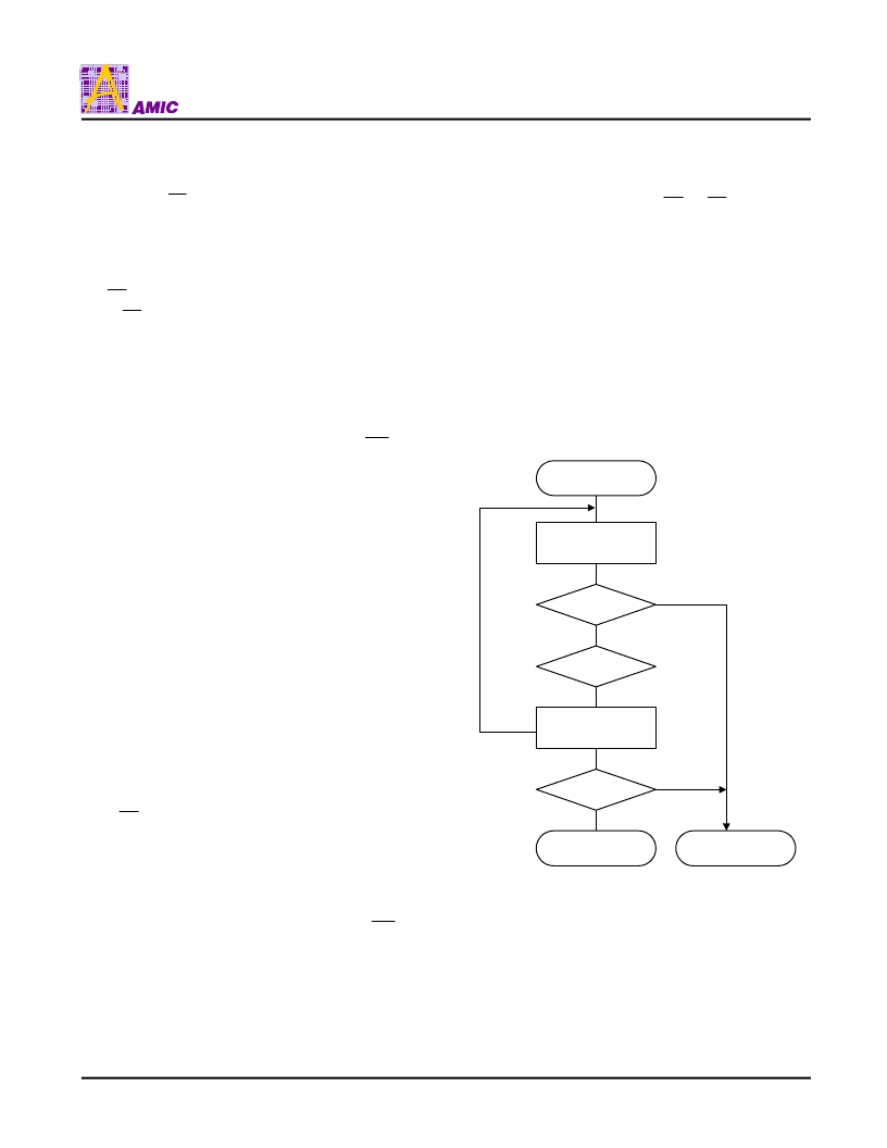
I/O
7
=Data
START
Read (I/O
0
to I/O
7
)
An=Valid Address
I/O
7
=Data
FAIL
No
Read (I/O
0
to I/O
7
)
An=Valid Address
I/O
5
=1
Yes
No
PASS
Yes
Yes
Figure 6. Data Polling Flow Chart
No
相关PDF资料 |
PDF描述 |
|---|---|
| A29L040SERIES | 512K X 8 Bit CMOS 3.0 Volt-only. Uniform Sector Flash Memory |
| A29L160SERIES | 2M X 8 Bit / 1M X 16 Bit CMOS 3.0 Volt-only. Boot Sector Flash Memory |
| A29L400SERIES | 512K X 8 Bit / 256K X 16 Bit CMOS 3.0 Volt-only. Boot Sector Flash Memory |
| A29L800SERIES | 1M X 8 Bit / 512K X 16 Bit CMOS 3.0 Volt-only. Boot Sector Flash Memory |
| A31-1 | 10 TO 2000 MHz CECASCADABLE AMPLIFIER |
相关代理商/技术参数 |
参数描述 |
|---|---|
| A29DL324TG-120 | 制造商:AMICC 制造商全称:AMIC Technology 功能描述:32 Megabit (4M x 8-Bit/2M x 16-Bit) CMOS 3.0 Volt-only, Simultaneous Operation Flash Memory |
| A29DL324TG-70 | 制造商:AMICC 制造商全称:AMIC Technology 功能描述:32 Megabit (4M x 8-Bit/2M x 16-Bit) CMOS 3.0 Volt-only, Simultaneous Operation Flash Memory |
| A29DL324TG-80 | 制造商:AMICC 制造商全称:AMIC Technology 功能描述:32 Megabit (4M x 8-Bit/2M x 16-Bit) CMOS 3.0 Volt-only, Simultaneous Operation Flash Memory |
| A29DL324TG-90 | 制造商:AMICC 制造商全称:AMIC Technology 功能描述:32 Megabit (4M x 8-Bit/2M x 16-Bit) CMOS 3.0 Volt-only, Simultaneous Operation Flash Memory |
| A29DL324TV-120 | 制造商:AMICC 制造商全称:AMIC Technology 功能描述:32 Megabit (4M x 8-Bit/2M x 16-Bit) CMOS 3.0 Volt-only, Simultaneous Operation Flash Memory |
发布紧急采购,3分钟左右您将得到回复。