参数资料
| 型号: | ACS8946T |
| 厂商: | Semtech |
| 文件页数: | 40/40页 |
| 文件大小: | 0K |
| 描述: | IC JITTER ATT MULT PLL 48-QFN |
| 标准包装: | 1 |
| 类型: | 时钟/频率发生器,多路复用器 |
| PLL: | 是 |
| 主要目的: | 以太网,SONET/SDH |
| 输入: | LVPECL |
| 输出: | CML,LVPECL |
| 电路数: | 1 |
| 比率 - 输入:输出: | 2:4 |
| 差分 - 输入:输出: | 是/是 |
| 频率 - 最大: | 625MHz |
| 电源电压: | 3.135 V ~ 3.465 V |
| 工作温度: | -40°C ~ 85°C |
| 安装类型: | 表面贴装 |
| 封装/外壳: | 48-VFQFN 裸露焊盘 |
| 供应商设备封装: | 48-QFN(7x7) |
| 包装: | 托盘 |
第1页第2页第3页第4页第5页第6页第7页第8页第9页第10页第11页第12页第13页第14页第15页第16页第17页第18页第19页第20页第21页第22页第23页第24页第25页第26页第27页第28页第29页第30页第31页第32页第33页第34页第35页第36页第37页第38页第39页当前第40页
ADVANCED COMMUNICATIONS
FINAL
DATASHEET
Revision 3/November 2006 Semtech Corp.
Page 9
www.semtech.com
ACS8946 JAM PLL
also possible using suitable passive components (see
Output clock rates at 19.44 MHz, 38.88 MHz, 77.76 MHz,
125.00 MHz, 155.52 MHz, 156.25 MHz, 311.04 MHz,
622.08 MHz or 625.00 MHz are selectable. Additionally,
odd number division of these frequencies up to divide-by-
15 can also be configured. Note that if odd number
division is used, the frequency adjustment factor will
apply to all outputs, adjusting all selected output
frequencies proportionally.
The output frequency of each output is determined by a
combination of the wiring of the configuration pins
CFG_IN[7:0] read at power-up, and state of the
asynchronously set RATE[2:1]A and RATE[2:1]B pins. The
user configures a set of “Available Rates” (four
frequencies that are available for selection at every Clock
Output) and then configures each output individually to
output one of these four rates. OUT1 and OUT2 are
asynchronously controllable allowing the output
frequency to be switched among the “Available Rates”
under control from the rate selection pins (RATE[2:1]A
and RATE[2:1]B).
To determine the correct wiring of configuration pins to
configure the device involves the use of several look-up
tables, and for completeness the datasheet includes all of
these, with worked examples (See “Configuration” on
page 13). However, to make configuring the device much
more simple than this description and look-up tables
suggest, Semtech provides a user-friendly Graphical User
Interface (GUI) software package to accompany the
ACS8946 in which the User enters the required I/O
frequencies, dividers settings etc. as required for a
particular application, and the GUI responds by displaying
the interconnections required to achieve that
configuration. Refer to the ACS8946 EVB Document and
associated software.
Unused outputs should be left floating with their
associated VDD connected to GND. For example, if OUT4
is not required, connect VDD04 to GND and leave OUT4N
and OUT4P unconnected.
Clock Multiplication
The ACS8946 provides options to multiply a 19.44 MHz
input by 2, 4, 8, 16, or 32 for standard SONET SDH spot
frequency configurations. 125.00 MHz dejittered output
for Gigabit Ethernet (GbE/10 GbE) is also supported if
125.00 MHz is provided as the input reference, and
156.25 MHz input (for 12.5 GbE) is also supported. These
rates are configured by the wiring of CFG_IN[3:2], see
If the input frequency used is a percentage away from the
configured spot frequency, then the resulting output
frequency will change by the same percentage. Refer
back to Table 5 for permitted input frequencies.
Note...GbE rates are not directly available as conversions from
SONET/SDH rates.
Voltage Controlled Oscillator
The internal VCO operates at 2.48832 GHz when the
device is configured for standard SONET/SDH spot
frequencies. The VCO frequency is divided down to the
selected rate giving a precise 50/50 balanced
mark/space ratio for the output. For 125.00 MHz
operation the VCO operates at 2.500 GHz.
Jitter Filtering
Input jitter is attenuated by the PLL with the frequency cut-
off point (Fc), at which jitter is either tracked or
attenuated, defined by the -3 dB point i.e. the position of
the first pole of the PLL loop filter. The bandwidth
(frequency at which the first pole occurs) is defined by the
For 19.44 MHz input, using a loop filter bandwidth of
2 kHz and damping factor of 1.2 gives:
High input jitter attenuation and roll off:
- 20 dB/decade from first loop filter pole, (Fc)
- 40 dB/decade from 2nd pole (typically 10 x Fc)
Jitter peaking is less than 1 dB (dependent on the
loop filter components)
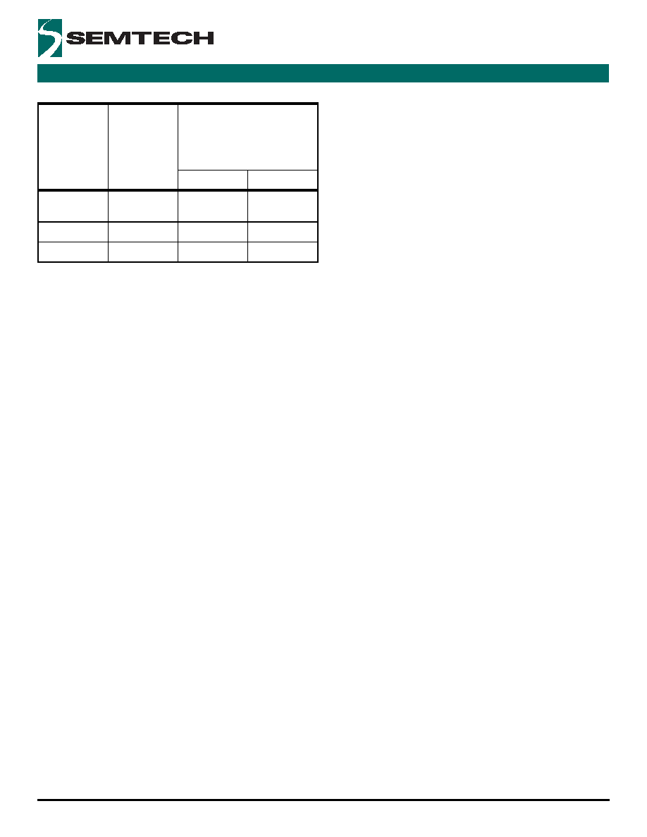
Table 5 Permitted Input Frequency Range
Selected Input
Spot
Frequency/
MHz
Selected FEC
Ratio (*or
Divider Ratio
using Odd
Divider)
Max and Min Permitted Input
Frequency Expressed as a
Percentage Above (+%) or Below
(-%) the Selected Input Spot
Frequency
+%
-%
19.44, 38.88
77.76, 155.52
1:1
12.0
3.0
125.00
5:4*
10.0
3.0
156.25
1:1
12.0
3.0
相关PDF资料 |
PDF描述 |
|---|---|
| ACS8947T | IC JITTER ATT MULT PLL 48-QFN |
| AD10200BZ | IC ADC DUAL 12BIT 68-CLCC |
| AD10242BZ | IC ADC DUAL 12BIT 68-CLCC |
| AD10465BZ | IC ADC DUAL 14BIT 68-CLCC |
| AD13280AZ | IC ADC 12BIT 68CLCC |
相关代理商/技术参数 |
参数描述 |
|---|---|
| ACS8947T | 功能描述:IC JITTER ATT MULT PLL 48-QFN RoHS:是 类别:集成电路 (IC) >> 时钟/计时 - 专用 系列:- 标准包装:1,500 系列:- 类型:时钟缓冲器/驱动器 PLL:是 主要目的:- 输入:- 输出:- 电路数:- 比率 - 输入:输出:- 差分 - 输入:输出:- 频率 - 最大:- 电源电压:3.3V 工作温度:0°C ~ 70°C 安装类型:表面贴装 封装/外壳:28-SSOP(0.209",5.30mm 宽) 供应商设备封装:28-SSOP 包装:带卷 (TR) 其它名称:93786AFT |
| ACS9010 | 制造商:未知厂家 制造商全称:未知厂家 功能描述:Optoelectronic |
| ACS9510/50EVB | 制造商:Semtech Corporation 功能描述: |
| ACS9510EVB | 功能描述:EVALUATION BOARD FOR ACS9510 RoHS:是 类别:编程器,开发系统 >> 评估演示板和套件 系列:ToPSync™ 标准包装:1 系列:PCI Express® (PCIe) 主要目的:接口,收发器,PCI Express 嵌入式:- 已用 IC / 零件:DS80PCI800 主要属性:- 次要属性:- 已供物品:板 |
| ACS9510T | 制造商:Semtech Corporation 功能描述: |
发布紧急采购,3分钟左右您将得到回复。