参数资料
| 型号: | AD5422BREZ |
| 厂商: | Analog Devices Inc |
| 文件页数: | 31/44页 |
| 文件大小: | 0K |
| 描述: | IC DAC 16BIT 1CH 24TSSOP |
| 产品培训模块: | Power Line Monitoring Data Converter Fundamentals DAC Architectures |
| 设计资源: | 16-Bit Fully Isolated Output Module Using AD5422 and ADuM1401 (CN0065) Simplified 16-Bit Voltage Output and 4 mA-to-20 mA Output Solution Using AD5422 (CN0077) |
| 标准包装: | 62 |
| 设置时间: | 25µs |
| 位数: | 16 |
| 数据接口: | MICROWIRE?,串行,SPI? |
| 转换器数目: | 1 |
| 电压电源: | 模拟和数字,双 ± |
| 功率耗散(最大): | 950mW |
| 工作温度: | -40°C ~ 85°C |
| 安装类型: | 表面贴装 |
| 封装/外壳: | 24-TSSOP(0.173",4.40mm)裸露焊盘 |
| 供应商设备封装: | 24-TSSOP 裸露焊盘 |
| 包装: | 管件 |
| 输出数目和类型: | 1 电流,单极;1 电流,双极;1 电压,单极;1 电压,双极 |
| 采样率(每秒): | 40k |
| 产品目录页面: | 782 (CN2011-ZH PDF) |
第1页第2页第3页第4页第5页第6页第7页第8页第9页第10页第11页第12页第13页第14页第15页第16页第17页第18页第19页第20页第21页第22页第23页第24页第25页第26页第27页第28页第29页第30页当前第31页第32页第33页第34页第35页第36页第37页第38页第39页第40页第41页第42页第43页第44页
Data Sheet
AD5412/AD5422
Rev. I | Page 37 of 44
APPLICATIONS INFORMATION
VOLTAGE AND CURRENT OUTPUT RANGES ON
THE SAME TERMINAL
The current and voltage output pins can be connected together.
A buffer amplifier is required however to prevent a current
leakage path through an internal 40k resistor on the +VSENSE pin,
when the device is in current output mode. In current mode the
VOUT pin is high impedance while in voltage output mode, the
IOUT pin is high impedance and will not affect the voltage
output. It is important that the external RSET be used in this
configuration, as depicted in Figure 77.
IOUT
AD5412/
AD5422
IOUT/VOUT
+VSENSE
–VSENSE
VOUT
RSET
OP07/OP184
06996-
071
Figure 77. IOUT and VOUT Connected Together
DRIVING INDUCTIVE LOADS
When driving inductive or poorly defined loads, connect a
0.01 F capacitor between IOUT and GND. This ensures stability
with loads above 50 mH. There is no maximum capacitance
limit. The capacitive component of the load may cause slower
settling. The digital slew rate control feature may also prove
useful in this situation.
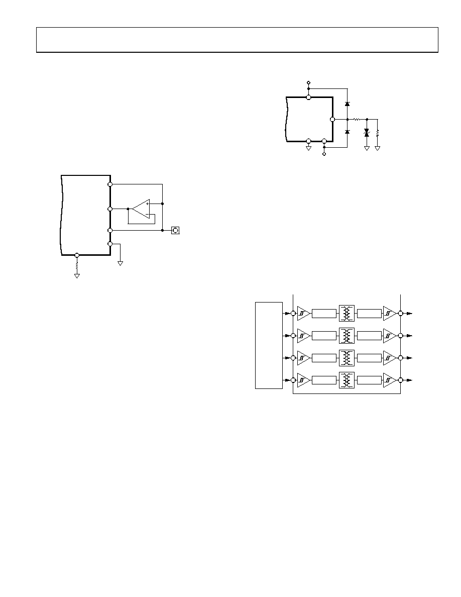
TRANSIENT VOLTAGE PROTECTION
prevent damage from normal handling. The industrial control
environment can, however, subject I/O circuits to much higher
high voltage transients, external power diodes and a surge
current limiting resistor are required, as shown in Figure 78.
The constraint on the resistor value is that, during normal
operation, the output level at IOUT must remain within its voltage
compliance limit of AVDD – 2.5 V, and the two protection diodes
and resistor must have appropriate power ratings. Further
protection can be provided with transient voltage suppressors or
transorbs; these are available as both unidirectional suppressors
(protect against positive high voltage transients) and
bidirectional suppressors (protect against both positive and
negative high voltage transients) and are available in a wide
range of standoff and breakdown voltage ratings. It is
recommended that all field connected nodes be protected.
AVDD
IOUT
RLOAD
RP
AVDD
AD5412/
AD5422
GND
AVSS
06996-
064
Figure 78. Output Transient Voltage Protection
GALVANICALLY ISOLATED INTERFACE
In many process control applications, it is necessary to provide
an isolation barrier between the controller and the unit being
controlled to protect and isolate the controlling circuitry from
any hazardous common-mode voltages that may occur. The
iCoupler products from Analog Devices, Inc., provide voltage
isolation in excess of 2.5 kV. The serial loading structure of the
because the number of interface lines is kept to a minimum.
AD5422 using an ADuM1400. For further information, visit
ENCODE
SERIAL
CLOCK IN
CONTROLLER
ADuM14001
SERIAL
DATA OUT
SYNC OUT
CONTROL
OUT
DECODE
TO
SCLK
TO
SDIN
TO
LATCH
TO
CLEAR
VIA
VOA
ENCODE
DECODE
VIB
VOB
ENCODE
DECODE
VIC
VOC
ENCODE
DECODE
VID
VOD
06996-
065
1ADDITIONAL PINS OMITTED FOR CLARITY.
Figure 79. Isolated Interface
MICROPROCESSOR INTERFACING
bus that uses a protocol compatible with microcontrollers and
DSP processors. The communications channel is a 3-wire
minimum interface consisting of a clock signal, a data signal,
word with data valid on the rising edge of SCLK.
For all interfaces, the DAC output update is initiated on the
rising edge of LATCH. The contents of the registers can be
read using the readback function.
相关PDF资料 |
PDF描述 |
|---|---|
| VI-BTT-MY-F4 | CONVERTER MOD DC/DC 6.5V 50W |
| VE-J4D-MZ-F2 | CONVERTER MOD DC/DC 85V 25W |
| VE-B4Z-MU-F1 | CONVERTER MOD DC/DC 2V 80W |
| VI-BTT-MY-F3 | CONVERTER MOD DC/DC 6.5V 50W |
| LTC1454IS#PBF | IC D/A CONV 12BIT R-R DUAL16SOIC |
相关代理商/技术参数 |
参数描述 |
|---|---|
| AD5422BREZ-REEL | 功能描述:IC DAC 16BIT 1CH SRL INP 24TSSOP RoHS:是 类别:集成电路 (IC) >> 数据采集 - 数模转换器 系列:- 标准包装:47 系列:- 设置时间:2µs 位数:14 数据接口:并联 转换器数目:1 电压电源:单电源 功率耗散(最大):55µW 工作温度:-40°C ~ 85°C 安装类型:表面贴装 封装/外壳:28-SSOP(0.209",5.30mm 宽) 供应商设备封装:28-SSOP 包装:管件 输出数目和类型:1 电流,单极;1 电流,双极 采样率(每秒):* |
| AD5424 | 制造商:AD 制造商全称:Analog Devices 功能描述:Dual 8-,10-,12-Bit High Bandwidth Multiplying DACs with Serial Interface |
| AD5424_1 | 制造商:AD 制造商全称:Analog Devices 功能描述:8-/10-/12-Bit, High Bandwidth Multiplying DACs with Parallel Interface |
| AD5424BRU | 制造商:Analog Devices 功能描述:DAC SGL R-2R 8BIT 16TSSOP - Bulk |
| AD5424YCP | 制造商:Analog Devices 功能描述:DAC 1-CH R-2R 8-bit 20-Pin LFCSP EP 制造商:Rochester Electronics LLC 功能描述:8-BIT IOUT DAC PARELLED INT/FACE I.C. - Bulk |
发布紧急采购,3分钟左右您将得到回复。