参数资料
| 型号: | AD5422BREZ |
| 厂商: | Analog Devices Inc |
| 文件页数: | 32/44页 |
| 文件大小: | 0K |
| 描述: | IC DAC 16BIT 1CH 24TSSOP |
| 产品培训模块: | Power Line Monitoring Data Converter Fundamentals DAC Architectures |
| 设计资源: | 16-Bit Fully Isolated Output Module Using AD5422 and ADuM1401 (CN0065) Simplified 16-Bit Voltage Output and 4 mA-to-20 mA Output Solution Using AD5422 (CN0077) |
| 标准包装: | 62 |
| 设置时间: | 25µs |
| 位数: | 16 |
| 数据接口: | MICROWIRE?,串行,SPI? |
| 转换器数目: | 1 |
| 电压电源: | 模拟和数字,双 ± |
| 功率耗散(最大): | 950mW |
| 工作温度: | -40°C ~ 85°C |
| 安装类型: | 表面贴装 |
| 封装/外壳: | 24-TSSOP(0.173",4.40mm)裸露焊盘 |
| 供应商设备封装: | 24-TSSOP 裸露焊盘 |
| 包装: | 管件 |
| 输出数目和类型: | 1 电流,单极;1 电流,双极;1 电压,单极;1 电压,双极 |
| 采样率(每秒): | 40k |
| 产品目录页面: | 782 (CN2011-ZH PDF) |
第1页第2页第3页第4页第5页第6页第7页第8页第9页第10页第11页第12页第13页第14页第15页第16页第17页第18页第19页第20页第21页第22页第23页第24页第25页第26页第27页第28页第29页第30页第31页当前第32页第33页第34页第35页第36页第37页第38页第39页第40页第41页第42页第43页第44页
AD5412/AD5422
Data Sheet
Rev. I | Page 38 of 44
LAYOUT GUIDELINES
In any circuit where accuracy is important, careful consideration of
the power supply and ground return layout helps to ensure the
rated performance. Design the printed circuit board (PCB) on
digital sections are separated and confined to certain areas of the
devices require an analog ground-to-digital ground connection,
make the connection at one point only. Establish the star ground
point as close as possible to the device.
10 F in parallel with 0.1 F on each supply located as close to
the package as possible, ideally right up against the device. The
10 F capacitors are the tantalum bead type. The 0.1 F capacitor
should have low effective series resistance (ESR) and low effective
series inductance (ESI), such as the common ceramic types,
which provide a low impedance path to ground at high frequencies
to handle transient currents due to internal logic switching.
large a trace as possible to provide low impedance paths and reduce
the effects of glitches on the power supply line. Fast switching
signals such as clocks should be shielded with a digital ground
to avoid radiating noise to other parts of the board. Never run these
near the reference inputs. A ground line routed between the SDIN
and SCLK lines helps reduce crosstalk between them (this is not
required on a multilayer board that has a separate ground plane,
but separating the lines helps). It is essential to minimize noise
on the REFIN line because it couples through to the DAC output.
Avoid crossover of digital and analog signals. Traces on
opposite sides of the PCB should run at right angles to each
other. This reduces the effects of feed through the board. A
microstrip technique is by far the best but not always possible
with a double-sided board. In this technique, the component
side of the board is dedicated to the ground plane, and signal
traces are placed on the solder side.
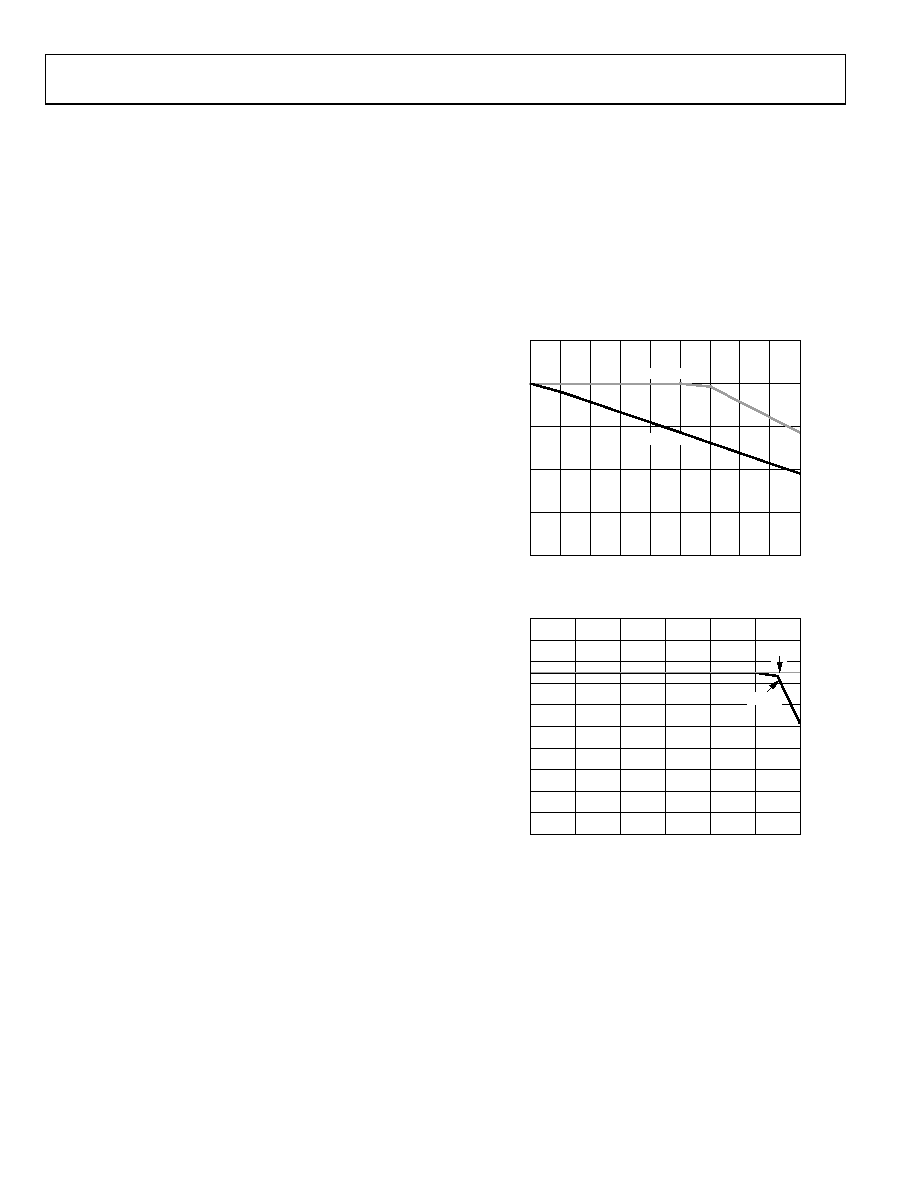
THERMAL AND SUPPLY CONSIDERATIONS
junction temperature of 125°C. It is important that the devices
not be operated under conditions that cause the junction
temperature to exceed this value. Excessive junction tempera-
maximum AVDD while driving the maximum current (24 mA)
directly to ground. In this case, control the ambient temperature
or reduce AVDD. The conditions depend on the device package.
At the maximum ambient temperature of 85°C, the 24-lead TSSOP
package can dissipate 1.14 mW, and the 40-lead LFCSP package
can dissipate 1.21 W.
To ensure that the junction temperature does not exceed 125°C
while driving the maximum current of 24 mA directly into ground
(also adding an on-chip current of 3 mA), reduce AVDD from the
maximum rating to ensure that the package is not required to
dissipate more power than previously stated (see Table 25,
Figure 80, and Figure 81).
0
0.5
1.0
1.5
2.0
2.5
40
45
50
55
60
65
70
75
80
85
AMBIENT TEMPERATURE (°C)
PO
W
ER
D
ISSI
PA
T
IO
N
(W
)
LFCSP
TSSOP
06996-
066
Figure 80. Maximum Power Dissipation vs. Ambient Temperature
25
27
29
31
33
35
37
39
41
43
45
25
35
45
55
65
75
85
AMBIENT TEMPERATURE (°C)
SU
PPL
Y
VO
L
T
A
G
E
(V)
06996-
067
TSSOP
LFCSP
Figure 81. Maximum Supply Voltage vs. Ambient Temperature
相关PDF资料 |
PDF描述 |
|---|---|
| VI-BTT-MY-F4 | CONVERTER MOD DC/DC 6.5V 50W |
| VE-J4D-MZ-F2 | CONVERTER MOD DC/DC 85V 25W |
| VE-B4Z-MU-F1 | CONVERTER MOD DC/DC 2V 80W |
| VI-BTT-MY-F3 | CONVERTER MOD DC/DC 6.5V 50W |
| LTC1454IS#PBF | IC D/A CONV 12BIT R-R DUAL16SOIC |
相关代理商/技术参数 |
参数描述 |
|---|---|
| AD5422BREZ-REEL | 功能描述:IC DAC 16BIT 1CH SRL INP 24TSSOP RoHS:是 类别:集成电路 (IC) >> 数据采集 - 数模转换器 系列:- 标准包装:47 系列:- 设置时间:2µs 位数:14 数据接口:并联 转换器数目:1 电压电源:单电源 功率耗散(最大):55µW 工作温度:-40°C ~ 85°C 安装类型:表面贴装 封装/外壳:28-SSOP(0.209",5.30mm 宽) 供应商设备封装:28-SSOP 包装:管件 输出数目和类型:1 电流,单极;1 电流,双极 采样率(每秒):* |
| AD5424 | 制造商:AD 制造商全称:Analog Devices 功能描述:Dual 8-,10-,12-Bit High Bandwidth Multiplying DACs with Serial Interface |
| AD5424_1 | 制造商:AD 制造商全称:Analog Devices 功能描述:8-/10-/12-Bit, High Bandwidth Multiplying DACs with Parallel Interface |
| AD5424BRU | 制造商:Analog Devices 功能描述:DAC SGL R-2R 8BIT 16TSSOP - Bulk |
| AD5424YCP | 制造商:Analog Devices 功能描述:DAC 1-CH R-2R 8-bit 20-Pin LFCSP EP 制造商:Rochester Electronics LLC 功能描述:8-BIT IOUT DAC PARELLED INT/FACE I.C. - Bulk |
发布紧急采购,3分钟左右您将得到回复。