- 您现在的位置:买卖IC网 > PDF目录1979 > AD5744RCSUZ-REEL7 (Analog Devices Inc)IC DAC QUAD 14BIT 1LSB 32TQFP PDF资料下载
参数资料
| 型号: | AD5744RCSUZ-REEL7 |
| 厂商: | Analog Devices Inc |
| 文件页数: | 14/32页 |
| 文件大小: | 0K |
| 描述: | IC DAC QUAD 14BIT 1LSB 32TQFP |
| 产品培训模块: | Data Converter Fundamentals DAC Architectures |
| 产品变化通告: | AD5764(R), AD5744R Product Change 04/Sept/2009 |
| 标准包装: | 500 |
| 设置时间: | 10µs |
| 位数: | 14 |
| 数据接口: | 串行 |
| 转换器数目: | 4 |
| 电压电源: | 模拟和数字,双 ± |
| 功率耗散(最大): | 387mW |
| 工作温度: | -40°C ~ 85°C |
| 安装类型: | 表面贴装 |
| 封装/外壳: | 32-TQFP |
| 供应商设备封装: | 32-TQFP(7x7) |
| 包装: | 带卷 (TR) |
| 输出数目和类型: | 4 电压,双极 |
| 采样率(每秒): | * |
第1页第2页第3页第4页第5页第6页第7页第8页第9页第10页第11页第12页第13页当前第14页第15页第16页第17页第18页第19页第20页第21页第22页第23页第24页第25页第26页第27页第28页第29页第30页第31页第32页
Data Sheet
AD5744R
Rev. E | Page 21 of 32
THEORY OF OPERATION
The AD5744R is a quad, 14-bit, serial input, bipolar voltage output
DAC that operates from supply voltages of ±11.4 V to ±16.5 V and
has a buffered output voltage of up to ±10.5263 V. Data is written to
the AD5744R in a 24-bit word format via a 3-wire serial interface.
The AD5744R also offers an SDO pin that is available for daisy
chaining or readback.
The AD5744R incorporates a power-on reset circuit that ensures
that the data registers are loaded with 0x0000 at power-up. The
AD5744R features a digital I/O port that can be programmed via
the serial interface, an analog die temperature sensor, on-chip
10 ppm/°C voltage reference, on-chip reference buffers, and per
channel digital gain and offset registers.
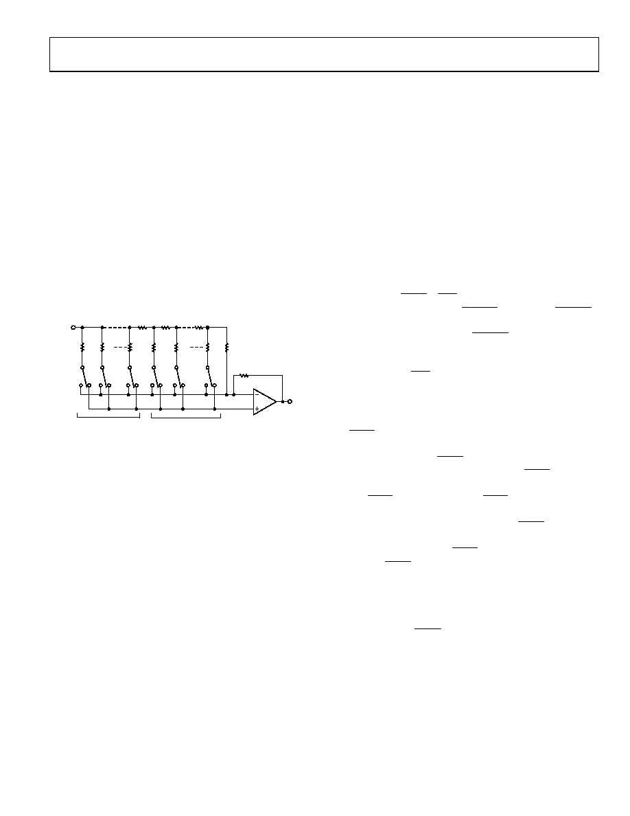
DAC ARCHITECTURE
The DAC architecture of the AD5744R consists of a 14-bit current
mode segmented R-2R DAC. The simplified circuit diagram for
the DAC section is shown in Figure 39.
0
606
5-
060
2R
E15
VREF
2R
E14
E1
2R
S11
RR
R
2R
S10
2R
12-BIT, R-2R LADDER
4 MSBs DECODED INTO
15 EQUAL SEGMENTS
VOUTx
2R
S0
2R
AGNDx
R/8
IOUT
Figure 39. DAC Ladder Structure
The four MSBs of the 14-bit data-word are decoded to drive
15 switches, E1 to E15. Each of these switches connects one of
the 15 matched resistors to either AGNDx or IOUT. The remaining
12 bits of the data-word drive Switch S0 to Switch S11 of the 12-bit
R-2R ladder network.
REFERENCE BUFFERS
The AD5744R can operate with either an external or an internal
reference. The reference inputs (REFAB and REFCD) have an
input range of up to 7 V. This input voltage is then used to provide
a buffered positive and negative reference for the DAC cores.
The positive reference is given by
+VREF = 2 × VREFIN
The negative reference to the DAC cores is given by
VREF = 2 × VREFIN
These positive and negative reference voltages (along with the
gain register values) define the output ranges of the DACs.
SERIAL INTERFACE
The AD5744R is controlled over a versatile 3-wire serial interface
that operates at clock rates of up to 30 MHz and is compatible
with SPI, QSPI, MICROWIRE, and DSP standards.
Input Shift Register
The input shift register is 24 bits wide. Data is loaded into the
device, MSB first, as a 24-bit word under the control of a serial
clock input, SCLK. The input register consists of a read/write bit,
a reserved bit that must be set to 0, three register select bits, three
DAC address bits, and 16 data bits, as shown in Table 9. The timing
diagram for this operation is shown in Figure 2.
Upon power-up, the data registers are loaded with zero code
(0x0000), and the outputs are clamped to 0 V via a low impedance
path. The outputs can be updated with the zero code value by
asserting either LDAC or CLR. The corresponding output voltage
depends on the state of the BIN/2sCOMP pin. If the BIN/2sCOMP
pin is tied to DGND, the data coding is twos complement and the
outputs update to 0 V. If the BIN/2sCOMP pin is tied to DVCC,
the data coding is offset binary and the outputs update to negative
full scale. To have the outputs power-up with zero code loaded
to the outputs, the CLR pin should be held low during power-up.
Standalone Operation
The serial interface works with both a continuous and noncon-
tinuous serial clock. A continuous SCLK source can be used only
if SYNC is held low for the correct number of clock cycles. In gated
clock mode, a burst clock containing the exact number of clock
cycles must be used, and SYNC must be taken high after the final
clock to latch the data. The first falling edge of SYNC starts the
write cycle. Exactly 24 falling clock edges must be applied to SCLK
before SYNC is brought high again. If SYNC is brought high before
the 24th falling SCLK edge, the data written is invalid. If more
than 24 falling SCLK edges are applied before SYNC is brought
high, the input data is also invalid. The input register addressed is
updated on the rising edge of SYNC. For another serial transfer to
take place, SYNC must be brought low again. After the end of
the serial data transfer, data is automatically transferred from the
input shift register to the addressed register.
When the data has been transferred into the chosen register of
the addressed DAC, all data registers and outputs can be
updated by taking LDAC low.
相关PDF资料 |
PDF描述 |
|---|---|
| AD574AKPZ-REEL | IC ADC 12BIT W/REF/CLK 28-PLCC |
| AD5752AREZ | IC DAC DUAL 16BIT SERIAL 24TSSOP |
| AD5752RBREZ-REEL7 | IC DAC DUAL 16BIT SERIAL 24TSSOP |
| AD5754BREZ-REEL7 | IC DAC 16BIT DSP/SRL 24TSSOP |
| AD5755-1ACPZ | IC DAC 16BIT SERIAL 64LFCSP |
相关代理商/技术参数 |
参数描述 |
|---|---|
| AD5748 | 制造商:AD 制造商全称:Analog Devices 功能描述:Industrial Current/Voltage Output Driver with Programmable Ranges |
| AD5748_1 | 制造商:AD 制造商全称:Analog Devices 功能描述:Industrial Current/Voltage Output Driver with Programmable Ranges |
| AD5748ACPZ | 功能描述:IC I/V OUTPUT DRIVER 32LFCSP RoHS:是 类别:集成电路 (IC) >> Linear - Amplifiers - Instrumentation 系列:- 标准包装:73 系列:Over-The-Top® 放大器类型:通用 电路数:4 输出类型:满摆幅 转换速率:0.07 V/µs 增益带宽积:200kHz -3db带宽:- 电流 - 输入偏压:1nA 电压 - 输入偏移:285µV 电流 - 电源:50µA 电流 - 输出 / 通道:25mA 电压 - 电源,单路/双路(±):2 V ~ 44 V,±1 V ~ 22 V 工作温度:-40°C ~ 85°C 安装类型:表面贴装 封装/外壳:16-WFDFN 裸露焊盘 供应商设备封装:16-DFN-EP(5x3) 包装:管件 |
| AD5748ACPZ-RL7 | 功能描述:IC I/V OUTPUT DRIVER 32LFCSP RoHS:是 类别:集成电路 (IC) >> Linear - Amplifiers - Instrumentation 系列:- 产品培训模块:Lead (SnPb) Finish for COTS Obsolescence Mitigation Program 标准包装:1 系列:- 放大器类型:电流检测 电路数:1 输出类型:- 转换速率:- 增益带宽积:125kHz -3db带宽:- 电流 - 输入偏压:- 电压 - 输入偏移:100µV 电流 - 电源:1.1µA 电流 - 输出 / 通道:- 电压 - 电源,单路/双路(±):- 工作温度:-40°C ~ 85°C 安装类型:表面贴装 封装/外壳:4-WFBGA,CSPBGA 供应商设备封装:4-UCSP(2x2) 包装:剪切带 (CT) 其它名称:MAX9634WERS+TCT |
| AD5749 | 制造商:AD 制造商全称:Analog Devices 功能描述:Industrial Current Out Driver, Single-Supply, 55 V Maximum Supply, Programmable Ranges |
发布紧急采购,3分钟左右您将得到回复。