- 您现在的位置:买卖IC网 > PDF目录1979 > AD5744RCSUZ-REEL7 (Analog Devices Inc)IC DAC QUAD 14BIT 1LSB 32TQFP PDF资料下载
参数资料
| 型号: | AD5744RCSUZ-REEL7 |
| 厂商: | Analog Devices Inc |
| 文件页数: | 15/32页 |
| 文件大小: | 0K |
| 描述: | IC DAC QUAD 14BIT 1LSB 32TQFP |
| 产品培训模块: | Data Converter Fundamentals DAC Architectures |
| 产品变化通告: | AD5764(R), AD5744R Product Change 04/Sept/2009 |
| 标准包装: | 500 |
| 设置时间: | 10µs |
| 位数: | 14 |
| 数据接口: | 串行 |
| 转换器数目: | 4 |
| 电压电源: | 模拟和数字,双 ± |
| 功率耗散(最大): | 387mW |
| 工作温度: | -40°C ~ 85°C |
| 安装类型: | 表面贴装 |
| 封装/外壳: | 32-TQFP |
| 供应商设备封装: | 32-TQFP(7x7) |
| 包装: | 带卷 (TR) |
| 输出数目和类型: | 4 电压,双极 |
| 采样率(每秒): | * |
第1页第2页第3页第4页第5页第6页第7页第8页第9页第10页第11页第12页第13页第14页当前第15页第16页第17页第18页第19页第20页第21页第22页第23页第24页第25页第26页第27页第28页第29页第30页第31页第32页
AD5744R
Data Sheet
Rev. E | Page 22 of 32
68HC11*
MISO
SYNC
SDIN
SCLK
MOSI
SCK
PC7
PC6
LDAC
SDO
SYNC
SCLK
LDAC
SDO
SYNC
SCLK
LDAC
SDO
SDIN
*ADDITIONAL PINS OMITTED FOR CLARITY.
AD5744R*
06
5-
06
1
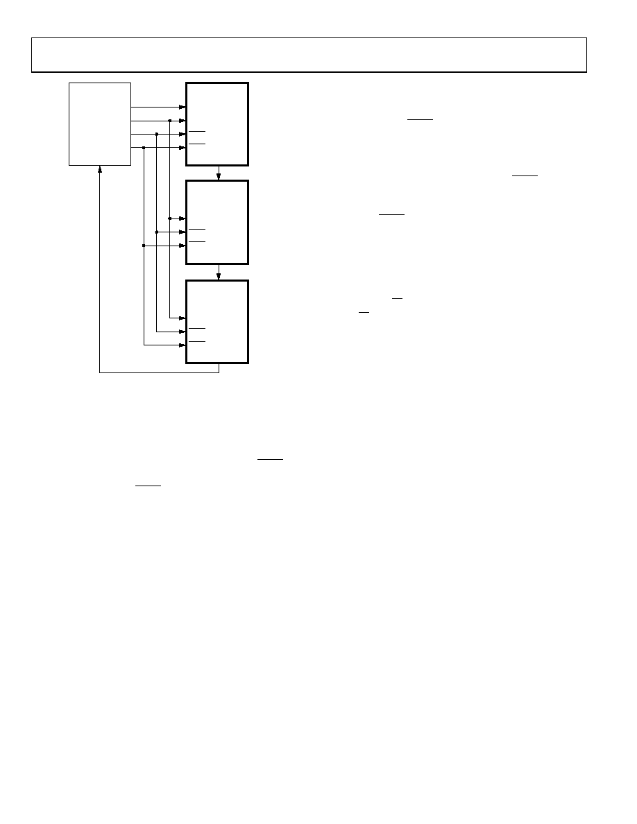
Figure 40. Daisy-Chaining the AD5744R
Daisy-Chain Operation
For systems that contain several devices, the SDO pin can be
used to daisy-chain several devices together. This daisy-chain
mode can be useful in system diagnostics and in reducing the
number of serial interface lines. The first falling edge of SYNC
starts the write cycle. The SCLK is continuously applied to the
input shift register when SYNC is low. If more than 24 clock
pulses are applied, the data ripples out of the shift register and
appears on the SDO line. This data is clocked out on the rising
edge of SCLK and is valid on the falling edge. By connecting the
SDO of the first device to the SDIN input of the next device in
the chain, a multidevice interface is constructed. Each device in
the system requires 24 clock pulses. Therefore, the total number
of clock cycles must equal 24n, where n is the total number of
AD5744R devices in the chain. When the serial transfer to all
devices is complete, SYNC is taken high. This latches the input
data in each device in the daisy chain and prevents any further
data from being clocked into the input shift register. The serial
clock can be a continuous or a gated clock.
A continuous SCLK source can be used only if SYNC is held
low for the correct number of clock cycles. In gated clock mode,
a burst clock containing the exact number of clock cycles must
be used, and SYNC must be taken high after the final clock to
latch the data.
Readback Operation
Before a readback operation is initiated, the SDO pin must be
enabled by writing to the function register and clearing the SDO
disable bit; this bit is cleared by default. Readback mode is invoked
by setting the R/W bit to 1 in the serial input register write.
With R/W set to 1, Bit A2 to Bit A0, in association with Bit REG2,
to Bit REG0, select the register to be read. The remaining data
bits in the write sequence are don’t care. During the next SPI write,
the data appearing on the SDO output contain the data from the
previously addressed register. For a read of a single register, the
NOP command can be used in clocking out the data from the
selected register on SDO. The readback diagram in
shows
the readback sequence. For example, to read back the fine gain
register of Channel A, implement the following sequence:
1.
Write 0xA0XXXX to the input register. This write configures
the AD5744R for read mode with the fine gain register of
Channel A selected. Note that all the data bits, DB15 to DB0,
are don’t care.
2.
Follow with a second write: an NOP condition, 0x00XXXX.
During this write, the data from the fine gain register is
clocked out on the SDO line; that is, data clocked out contains
the data from the fine gain register in Bit DB5 to Bit DB0.
相关PDF资料 |
PDF描述 |
|---|---|
| AD574AKPZ-REEL | IC ADC 12BIT W/REF/CLK 28-PLCC |
| AD5752AREZ | IC DAC DUAL 16BIT SERIAL 24TSSOP |
| AD5752RBREZ-REEL7 | IC DAC DUAL 16BIT SERIAL 24TSSOP |
| AD5754BREZ-REEL7 | IC DAC 16BIT DSP/SRL 24TSSOP |
| AD5755-1ACPZ | IC DAC 16BIT SERIAL 64LFCSP |
相关代理商/技术参数 |
参数描述 |
|---|---|
| AD5748 | 制造商:AD 制造商全称:Analog Devices 功能描述:Industrial Current/Voltage Output Driver with Programmable Ranges |
| AD5748_1 | 制造商:AD 制造商全称:Analog Devices 功能描述:Industrial Current/Voltage Output Driver with Programmable Ranges |
| AD5748ACPZ | 功能描述:IC I/V OUTPUT DRIVER 32LFCSP RoHS:是 类别:集成电路 (IC) >> Linear - Amplifiers - Instrumentation 系列:- 标准包装:73 系列:Over-The-Top® 放大器类型:通用 电路数:4 输出类型:满摆幅 转换速率:0.07 V/µs 增益带宽积:200kHz -3db带宽:- 电流 - 输入偏压:1nA 电压 - 输入偏移:285µV 电流 - 电源:50µA 电流 - 输出 / 通道:25mA 电压 - 电源,单路/双路(±):2 V ~ 44 V,±1 V ~ 22 V 工作温度:-40°C ~ 85°C 安装类型:表面贴装 封装/外壳:16-WFDFN 裸露焊盘 供应商设备封装:16-DFN-EP(5x3) 包装:管件 |
| AD5748ACPZ-RL7 | 功能描述:IC I/V OUTPUT DRIVER 32LFCSP RoHS:是 类别:集成电路 (IC) >> Linear - Amplifiers - Instrumentation 系列:- 产品培训模块:Lead (SnPb) Finish for COTS Obsolescence Mitigation Program 标准包装:1 系列:- 放大器类型:电流检测 电路数:1 输出类型:- 转换速率:- 增益带宽积:125kHz -3db带宽:- 电流 - 输入偏压:- 电压 - 输入偏移:100µV 电流 - 电源:1.1µA 电流 - 输出 / 通道:- 电压 - 电源,单路/双路(±):- 工作温度:-40°C ~ 85°C 安装类型:表面贴装 封装/外壳:4-WFBGA,CSPBGA 供应商设备封装:4-UCSP(2x2) 包装:剪切带 (CT) 其它名称:MAX9634WERS+TCT |
| AD5749 | 制造商:AD 制造商全称:Analog Devices 功能描述:Industrial Current Out Driver, Single-Supply, 55 V Maximum Supply, Programmable Ranges |
发布紧急采购,3分钟左右您将得到回复。