- 您现在的位置:买卖IC网 > PDF目录1979 > AD5744RCSUZ-REEL7 (Analog Devices Inc)IC DAC QUAD 14BIT 1LSB 32TQFP PDF资料下载
参数资料
| 型号: | AD5744RCSUZ-REEL7 |
| 厂商: | Analog Devices Inc |
| 文件页数: | 19/32页 |
| 文件大小: | 0K |
| 描述: | IC DAC QUAD 14BIT 1LSB 32TQFP |
| 产品培训模块: | Data Converter Fundamentals DAC Architectures |
| 产品变化通告: | AD5764(R), AD5744R Product Change 04/Sept/2009 |
| 标准包装: | 500 |
| 设置时间: | 10µs |
| 位数: | 14 |
| 数据接口: | 串行 |
| 转换器数目: | 4 |
| 电压电源: | 模拟和数字,双 ± |
| 功率耗散(最大): | 387mW |
| 工作温度: | -40°C ~ 85°C |
| 安装类型: | 表面贴装 |
| 封装/外壳: | 32-TQFP |
| 供应商设备封装: | 32-TQFP(7x7) |
| 包装: | 带卷 (TR) |
| 输出数目和类型: | 4 电压,双极 |
| 采样率(每秒): | * |
第1页第2页第3页第4页第5页第6页第7页第8页第9页第10页第11页第12页第13页第14页第15页第16页第17页第18页当前第19页第20页第21页第22页第23页第24页第25页第26页第27页第28页第29页第30页第31页第32页
AD5744R
Data Sheet
Rev. E | Page 26 of 32
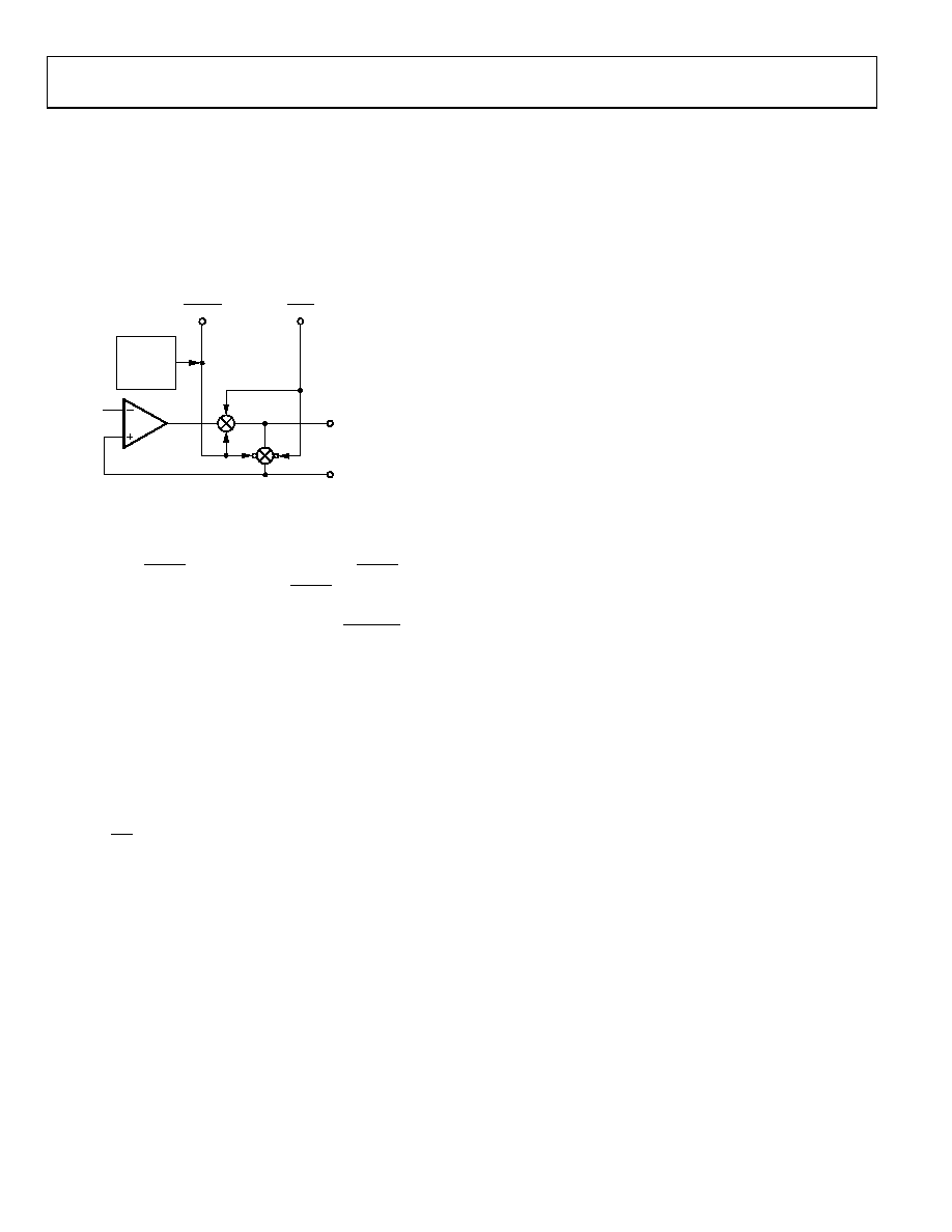
DESIGN FEATURES
ANALOG OUTPUT CONTROL
In many industrial process control applications, it is vital that
the output voltage be controlled during power-up and during
brownout conditions. When the supply voltages are changing,
the VOUTx pins are clamped to 0 V via a low impedance path.
To prevent the output amp from being shorted to 0 V during this
time, Transmission Gate G1 is also opened (see Figure 42).
G1
G2
RSTOUT
RSTIN
VOUTA
AGNDA
VOLTAGE
MONITOR
AND
CONTROL
06
5-
06
3
Figure 42. Analog Output Control Circuitry
These conditions are maintained until the power supplies stabilize
and a valid word is written to the data register. G2 then opens, and
G1 closes. Both transmission gates are also externally controllable
via the reset in (RSTIN) control input. For example, if RSTIN is
driven from a battery supervisor chip, the RSTIN input is driven
low to open G1 and close G2 on power-off or during a brownout.
Conversely, the on-chip voltage detector output (RSTOUT) is
also available to the user to control other parts of the system.
The basic transmission gate functionality is shown in
.
PROGRAMMABLE SHORT-CIRCUIT PROTECTION
The short-circuit current (ISC) of the output amplifiers can be
programmed by inserting an external resistor between the ISCC
pin and the PGND pin. The programmable range for the current is
500 μA to 10 mA, corresponding to a resistor range of 120 kΩ to
6 kΩ . The resistor value is calculated as follows:
R ≈
SC
I
60
If the ISCC pin is left unconnected, the short-circuit current
limit defaults to 5 mA. It should be noted that limiting the short-
circuit current to a small value can affect the slew rate of the
output when driving into a capacitive load. Therefore, the value
of the short-circuit current that is programmed should take into
account the size of the capacitive load being driven.
DIGITAL I/O PORT
The AD5744R contains a 2-bit digital I/O port (D1 and D0).
These bits can be configured independently as inputs or outputs
and can be driven or have their values read back via the serial
interface. The I/O port signals are referenced to DVCC and DGND.
When configured as outputs, they can be used as control signals
to multiplexers or can be used to control calibration circuitry
elsewhere in the system. When configured as inputs, the logic
signals from limit switches, for example, can be applied to D0
and D1 and can be read back using the digital interface.
DIE TEMPERATURE SENSOR
The on-chip die temperature sensor provides a voltage output that
is linearly proportional to the Celsius temperature scale. Its nom-
inal output voltage is 1.47 V at 25°C die temperature, varying at
5 mV/°C, giving a typical output range of 1.175 V to 1.9 V over the
full temperature range. Its low output impedance and linear output
simplify interfacing to temperature control circuitry and analog-to-
digital converters (ADCs). The temperature sensor is provided
as more of a convenience than as a precise feature; it is intended
for indicating a die temperature change for recalibration purposes.
LOCAL GROUND OFFSET ADJUST
The AD5744R incorporates a local ground offset adjust feature
that, when enabled in the function register, adjusts the DAC
outputs for voltage differences between the individual DAC ground
pins and the REFGND pin, ensuring that the DAC output voltages
are always referenced to the local DAC ground pin. For example, if
the AGNDA pin is at +5 mV with respect to the REFGND pin, and
VOUTA is measured with respect to AGNDA, a 5 mV error
results, enabling the local ground offset adjust feature to adjust
VOUTA by +5 mV, thereby eliminating the error.
相关PDF资料 |
PDF描述 |
|---|---|
| AD574AKPZ-REEL | IC ADC 12BIT W/REF/CLK 28-PLCC |
| AD5752AREZ | IC DAC DUAL 16BIT SERIAL 24TSSOP |
| AD5752RBREZ-REEL7 | IC DAC DUAL 16BIT SERIAL 24TSSOP |
| AD5754BREZ-REEL7 | IC DAC 16BIT DSP/SRL 24TSSOP |
| AD5755-1ACPZ | IC DAC 16BIT SERIAL 64LFCSP |
相关代理商/技术参数 |
参数描述 |
|---|---|
| AD5748 | 制造商:AD 制造商全称:Analog Devices 功能描述:Industrial Current/Voltage Output Driver with Programmable Ranges |
| AD5748_1 | 制造商:AD 制造商全称:Analog Devices 功能描述:Industrial Current/Voltage Output Driver with Programmable Ranges |
| AD5748ACPZ | 功能描述:IC I/V OUTPUT DRIVER 32LFCSP RoHS:是 类别:集成电路 (IC) >> Linear - Amplifiers - Instrumentation 系列:- 标准包装:73 系列:Over-The-Top® 放大器类型:通用 电路数:4 输出类型:满摆幅 转换速率:0.07 V/µs 增益带宽积:200kHz -3db带宽:- 电流 - 输入偏压:1nA 电压 - 输入偏移:285µV 电流 - 电源:50µA 电流 - 输出 / 通道:25mA 电压 - 电源,单路/双路(±):2 V ~ 44 V,±1 V ~ 22 V 工作温度:-40°C ~ 85°C 安装类型:表面贴装 封装/外壳:16-WFDFN 裸露焊盘 供应商设备封装:16-DFN-EP(5x3) 包装:管件 |
| AD5748ACPZ-RL7 | 功能描述:IC I/V OUTPUT DRIVER 32LFCSP RoHS:是 类别:集成电路 (IC) >> Linear - Amplifiers - Instrumentation 系列:- 产品培训模块:Lead (SnPb) Finish for COTS Obsolescence Mitigation Program 标准包装:1 系列:- 放大器类型:电流检测 电路数:1 输出类型:- 转换速率:- 增益带宽积:125kHz -3db带宽:- 电流 - 输入偏压:- 电压 - 输入偏移:100µV 电流 - 电源:1.1µA 电流 - 输出 / 通道:- 电压 - 电源,单路/双路(±):- 工作温度:-40°C ~ 85°C 安装类型:表面贴装 封装/外壳:4-WFBGA,CSPBGA 供应商设备封装:4-UCSP(2x2) 包装:剪切带 (CT) 其它名称:MAX9634WERS+TCT |
| AD5749 | 制造商:AD 制造商全称:Analog Devices 功能描述:Industrial Current Out Driver, Single-Supply, 55 V Maximum Supply, Programmable Ranges |
发布紧急采购,3分钟左右您将得到回复。