- 您现在的位置:买卖IC网 > PDF目录1979 > AD5744RCSUZ-REEL7 (Analog Devices Inc)IC DAC QUAD 14BIT 1LSB 32TQFP PDF资料下载
参数资料
| 型号: | AD5744RCSUZ-REEL7 |
| 厂商: | Analog Devices Inc |
| 文件页数: | 16/32页 |
| 文件大小: | 0K |
| 描述: | IC DAC QUAD 14BIT 1LSB 32TQFP |
| 产品培训模块: | Data Converter Fundamentals DAC Architectures |
| 产品变化通告: | AD5764(R), AD5744R Product Change 04/Sept/2009 |
| 标准包装: | 500 |
| 设置时间: | 10µs |
| 位数: | 14 |
| 数据接口: | 串行 |
| 转换器数目: | 4 |
| 电压电源: | 模拟和数字,双 ± |
| 功率耗散(最大): | 387mW |
| 工作温度: | -40°C ~ 85°C |
| 安装类型: | 表面贴装 |
| 封装/外壳: | 32-TQFP |
| 供应商设备封装: | 32-TQFP(7x7) |
| 包装: | 带卷 (TR) |
| 输出数目和类型: | 4 电压,双极 |
| 采样率(每秒): | * |
第1页第2页第3页第4页第5页第6页第7页第8页第9页第10页第11页第12页第13页第14页第15页当前第16页第17页第18页第19页第20页第21页第22页第23页第24页第25页第26页第27页第28页第29页第30页第31页第32页
Data Sheet
AD5744R
Rev. E | Page 23 of 32
SIMULTANEOUS UPDATING VIA LDAC
TRANSFER FUNCTION
relationship for offset binary data coding and twos complement
data coding, respectively.
Depending on the status of both SYNC and LDAC, and after
data has been transferred into the input register of the DACs,
there are two ways to update the data registers and DAC outputs.
The output voltage expression for the AD5744R is given by
Individual DAC Updating
In individual DAC updating mode, LDAC is held low while data
is being clocked into the input shift register. The addressed
DAC output is updated on the rising edge of SYNC.
VOUT = 2 × VREFIN + 4 × VREFIN
384
,
16
D
where:
D is the decimal equivalent of the code loaded to the DAC.
VREFIN is the reference voltage applied at the REFAB and
REFCD pins.
Simultaneous Updating of All DACs
In simultaneous updating of all DACs mode, LDAC is held high
while data is being clocked into the input shift register. All DAC
outputs are updated by taking LDAC low any time after SYNC
has been taken high. The update then occurs on the falling edge
of LDAC.
ASYNCHRONOUS CLEAR (CLR)
CLR is a negative edge triggered clear that allows the outputs to
be cleared to either 0 V (twos complement coding) or negative full
scale (offset binary coding). It is necessary to maintain CLR low
for a minimum amount of time for the operation to complete
(see
). When the
CLR signal is returned high, the output
remains at the cleared value until a new value is programmed.
If CLR is at 0 V at power-on, all DAC outputs are updated with
the clear value. A clear can also be initiated through software by
writing the command of 0x04XXXX to the AD5744R.
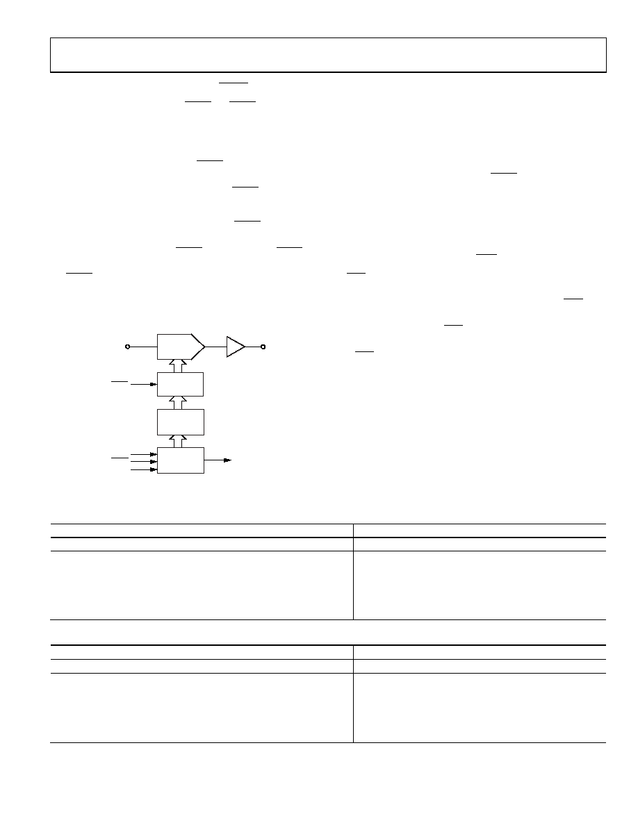
See Figure 41 for a simplified block diagram of the DAC load
circuitry.
VOUTx
DATA
REGISTER
INTERFACE
LOGIC
OUTPUT
I/V AMPLIFIER
LDAC
SDO
SDIN
14-BIT
DAC
REFAB, REFCD
SYNC
INPUT
REGISTER
SCLK
06
5-
0
62
Figure 41. Simplified Serial Interface of Input Loading Circuitry
for One DAC Channel
Table 7. Ideal Output Voltage to Input Code Relationship—Offset Binary Data Coding
Digital Input
Analog Output
MSB
LSB
VOUT
11
1111
+2 VREF × (8191/8192)
10
0000
0001
+2 VREF × (1/8192)
10
0000
0 V
01
1111
2 VREF × (1/8192)
00
0000
2 VREF × (8191/8192)
Table 8. Ideal Output Voltage to Input Code Relationship—Twos Complement Data Coding
Digital Input
Analog Output
MSB
LSB
VOUT
01
1111
+2 VREF × (8191/8192)
00
0000
0001
+2 VREF × (1/8192)
00
0000
0 V
11
1111
2 VREF × (1/8192)
10
0000
2 VREF × (8191/8192)
相关PDF资料 |
PDF描述 |
|---|---|
| AD574AKPZ-REEL | IC ADC 12BIT W/REF/CLK 28-PLCC |
| AD5752AREZ | IC DAC DUAL 16BIT SERIAL 24TSSOP |
| AD5752RBREZ-REEL7 | IC DAC DUAL 16BIT SERIAL 24TSSOP |
| AD5754BREZ-REEL7 | IC DAC 16BIT DSP/SRL 24TSSOP |
| AD5755-1ACPZ | IC DAC 16BIT SERIAL 64LFCSP |
相关代理商/技术参数 |
参数描述 |
|---|---|
| AD5748 | 制造商:AD 制造商全称:Analog Devices 功能描述:Industrial Current/Voltage Output Driver with Programmable Ranges |
| AD5748_1 | 制造商:AD 制造商全称:Analog Devices 功能描述:Industrial Current/Voltage Output Driver with Programmable Ranges |
| AD5748ACPZ | 功能描述:IC I/V OUTPUT DRIVER 32LFCSP RoHS:是 类别:集成电路 (IC) >> Linear - Amplifiers - Instrumentation 系列:- 标准包装:73 系列:Over-The-Top® 放大器类型:通用 电路数:4 输出类型:满摆幅 转换速率:0.07 V/µs 增益带宽积:200kHz -3db带宽:- 电流 - 输入偏压:1nA 电压 - 输入偏移:285µV 电流 - 电源:50µA 电流 - 输出 / 通道:25mA 电压 - 电源,单路/双路(±):2 V ~ 44 V,±1 V ~ 22 V 工作温度:-40°C ~ 85°C 安装类型:表面贴装 封装/外壳:16-WFDFN 裸露焊盘 供应商设备封装:16-DFN-EP(5x3) 包装:管件 |
| AD5748ACPZ-RL7 | 功能描述:IC I/V OUTPUT DRIVER 32LFCSP RoHS:是 类别:集成电路 (IC) >> Linear - Amplifiers - Instrumentation 系列:- 产品培训模块:Lead (SnPb) Finish for COTS Obsolescence Mitigation Program 标准包装:1 系列:- 放大器类型:电流检测 电路数:1 输出类型:- 转换速率:- 增益带宽积:125kHz -3db带宽:- 电流 - 输入偏压:- 电压 - 输入偏移:100µV 电流 - 电源:1.1µA 电流 - 输出 / 通道:- 电压 - 电源,单路/双路(±):- 工作温度:-40°C ~ 85°C 安装类型:表面贴装 封装/外壳:4-WFBGA,CSPBGA 供应商设备封装:4-UCSP(2x2) 包装:剪切带 (CT) 其它名称:MAX9634WERS+TCT |
| AD5749 | 制造商:AD 制造商全称:Analog Devices 功能描述:Industrial Current Out Driver, Single-Supply, 55 V Maximum Supply, Programmable Ranges |
发布紧急采购,3分钟左右您将得到回复。